

EV Group, or EVG, is a big name in making equipment for semiconductors. They’ve been around since 1980, and they’re known for coming up with new ways to make chips. From their early days, EVG has helped shape how microchips are put together, especially with things like wafer bonding. They’ve played a role in how many of the devices we use every day, like smartphones and cars, get their tiny brains. It’s pretty interesting how much impact one company can have on such a complex industry.
Key Takeaways
- EVG started in 1980 and has been a leader in semiconductor equipment ever since.
- They are especially good at wafer bonding, which is super important for making modern chips.
- EVG’s tools are used in making parts for things like phone cameras and car sensors.
- They’ve introduced many new technologies, including SmartView alignment and the GEMINI systems.
- EVG is working on solutions for future chip designs, like 3D integration and advanced packaging.
EVG’s Pioneering History
Founding And Early Innovations
So, EVG, right? They didn’t just pop up yesterday. Back in 1980, Aya Maria and DI Erich Thallner had this idea, a mix of bold thinking and a real dedication to making top-notch manufacturing systems. That’s what set the stage for EVG’s success. They weren’t afraid to try new things, and that’s paid off big time. It’s pretty cool to see how far they’ve come from those early days. I mean, think about it – they’ve been shaping the semiconductor industry for over four decades! Thomas Uhrmann is now VP of Sales, so it’s exciting to see where they go next.
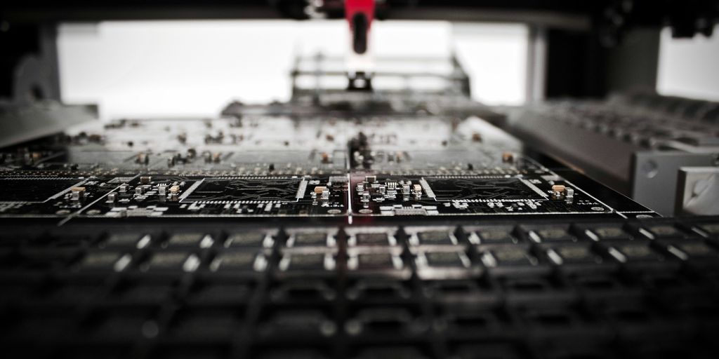
Revolutionizing Wafer Bonding
Okay, so wafer bonding might sound super technical, but trust me, it’s important. EVG didn’t just improve wafer bonding; they basically reinvented it. The separation of wafer alignment and bonding back in 1990? Game-changer. It became the industry standard. It’s like they figured out the secret sauce that everyone else was missing. This innovation allowed for more precise and efficient manufacturing processes. It’s one of those things that, looking back, you realize was a total turning point.
Market Leadership In MEMS Manufacturing
MEMS – Micro-Electro-Mechanical Systems – are everywhere these days, from your phone to your car. And EVG? They’re a big reason why. They introduced the first production wafer bonding system for volume MEMS manufacturing way back in 1992. That’s like setting the foundation for an entire industry. Because of that, they’re now a leader in wafer bonding systems. It’s not just about making the equipment; it’s about enabling the creation of all sorts of cool devices, like chips for blood analysis or DNA screening. They developed the world’s first double-side mask aligner with bottom-side microscopes, which enabled the widespread commercialization of MEMS products, in 1985.
Advanced Process Solutions By EVG
EVG isn’t just about making machines; they’re about providing complete solutions for complex manufacturing challenges. They’ve got a handle on several key areas, making them a go-to for companies pushing the boundaries of what’s possible in chip design and production. Let’s take a look at some of their core strengths.
Wafer Bonding Expertise
Wafer bonding is kind of EVG’s bread and butter. They’ve been doing it for a long time, and they’ve really refined the process. Their equipment allows for incredibly precise alignment and bonding of different materials, which is essential for creating advanced devices. Think about stacking layers of different semiconductors to create a more powerful or efficient chip – that’s where wafer bonding comes in. They offer a range of systems to handle different wafer sizes and materials, ensuring there’s a solution for pretty much any application. This is crucial for AI-powered wallet technology.
Lithography And Thin-Wafer Processing
Beyond bonding, EVG also has a strong presence in lithography. This is the process of printing patterns onto wafers, which is a critical step in creating the circuits that make up a chip. They’ve developed some innovative techniques, like maskless exposure, which allows for greater flexibility and faster turnaround times. Plus, they’re experts in handling thin wafers, which are becoming increasingly important for creating smaller, more efficient devices. Here’s a quick rundown of their lithography capabilities:
- Maskless Lithography: For rapid prototyping and low-volume production.
- UV Lithography: For high-resolution patterning.
- Nanoimprint Lithography (NIL): For replicating nanoscale structures.
Metrology Equipment And Applications
It’s not enough to just build the chips; you also need to be able to measure and inspect them to make sure they meet the required specifications. EVG offers a range of metrology equipment that can be used to characterize the properties of wafers and bonded stacks. This includes measuring things like thickness, stress, and alignment accuracy. This data is then used to optimize the manufacturing process and ensure that the final product meets the required standards. Think of it as quality control on a microscopic level. They also have application labs where they work with customers to develop and optimize processes for specific applications. They can help with everything from process development to equipment selection, making sure customers get the most out of their investment. They provide wafer bonding systems for volume MEMS manufacturing.
EVG’s Global Impact On Semiconductor Manufacturing
Enabling Next-Generation Chip Designs
EVG’s technology is a big deal when it comes to making advanced chips. Their equipment and processes are used to create the tiny structures on wafers that make up these chips. It’s not just about making things smaller; it’s about making them more efficient and powerful. Think about your smartphone – the reason it can do so much is because of the advanced chips inside, and EVG plays a role in making those chips a reality. They’re involved in everything from camera sensors to processors, helping to push the boundaries of what’s possible. The GaN Power Device Market is also impacted by EVG’s contributions.
Supporting 3D Integration And Advanced Packaging
3D integration is like building skyscrapers with chips – stacking them on top of each other to create more complex and powerful devices. EVG’s wafer bonding technology is key to making this happen. It’s not easy to stack these wafers perfectly, but EVG’s equipment allows manufacturers to do it with incredible precision. This is important for things like high-bandwidth memory and other advanced components. Advanced packaging is also crucial; it’s how these chips are connected and protected. EVG’s solutions help with this too, ensuring that the chips can function properly in all sorts of devices.
Global Customer And Partner Network
EVG isn’t just some company working in isolation. They have a huge network of customers and partners all over the world. This includes major semiconductor manufacturers, research institutions, and other technology companies. They have locations in North America and Asia, focused on delivering process wafer bonding expertise to their global R&D and production customer and partner base. This network allows them to stay at the forefront of innovation, working with others to develop new technologies and solutions. It also means that their technology is used in a wide range of applications, from smartphones to automotive systems to medical devices. They’re a key player in the global semiconductor ecosystem, helping to drive progress and innovation across the board.
Here’s a quick breakdown of their global presence:
- Subsidiaries: U.S., Japan, South Korea, China, Taiwan, Singapore
- Employees: Over 1600 worldwide
- Focus: Delivering process expertise globally
Key Innovations In Wafer Bonding
Wafer bonding is super important for making advanced semiconductors, and EVG has been at the forefront of pushing the tech forward. They’ve come up with some really cool stuff over the years that has helped to improve chip manufacturing. It’s not just about sticking wafers together; it’s about doing it with incredible precision and reliability. This is especially important as chips get more complex and smaller.
SmartView Alignment Technology
Okay, so imagine trying to stack two LEGO bricks together, but they’re microscopic and have to line up perfectly. That’s kind of what wafer alignment is like. EVG’s SmartView alignment technology makes this process way easier. It lets you see both wafers at the same time, so you can line them up with crazy accuracy. This is a big deal for things like 3D chip stacking, where even a tiny misalignment can mess everything up. It’s like having a superpower for aligning tiny things.
GEMINI Integrated Systems
Before GEMINI, wafer bonding was often a multi-step process using different machines. That’s slow and can introduce errors. The GEMINI system changed that by putting everything into one integrated platform. Think of it like an all-in-one printer, scanner, and copier, but for wafers. This means faster processing, better control, and less chance of something going wrong. It was the industry’s first integrated production wafer bonding system, launched way back in 2000, and it really set the standard for wafer bonding systems.
ComBond High-Vacuum Cluster Tool
This tool is all about getting really clean, strong bonds between wafers. The ComBond system uses a high vacuum environment to create bonds that are free of oxides and electrically conductive. This is especially useful for making engineered substrates and power devices. Basically, it lets you create new materials and devices that weren’t possible before. It’s like having a super-clean room where you can build things at the atomic level. This is critical for achieving the highest cell array efficiency in the industry.
EVG’s Role In Advanced Lithography
HERCULES NIL For High-Volume Manufacturing
EVG’s HERCULES NIL (Nanoimprint Lithography) system is designed for high-volume manufacturing. It’s all about getting those tiny patterns onto wafers quickly and accurately. This technology is especially useful for applications where you need really fine details, like in advanced optics or photonics. Think of it as a super-precise stamping machine for the nano-world. It helps reduce costs and increase throughput compared to traditional lithography methods.
LITHOSCALE And Maskless Exposure
LITHOSCALE is a big deal because it uses maskless exposure (MLE) technology. Instead of using a physical mask to project a pattern onto the wafer, MLE uses a digital pattern. This gives you a lot more flexibility in design and allows for faster prototyping. It’s like switching from a film projector to a digital projector – way easier to change the image. The Broadcom VMware acquisition could benefit from this technology.
IR LayerRelease For Ultra-Thin Stacking
IR LayerRelease is a pretty cool technology that lets you create ultra-thin chip stacks. Basically, you use infrared light to release a thin layer of material from a carrier wafer. This is super important for making smaller, more powerful devices. Imagine stacking layers of chips like pancakes to save space and improve performance. EVG’s EVG®880 LayerRelease™ system even won an award for it! This is key for wafer bonding in advanced packaging.
EVG’s Contribution To Diverse Applications
EVG’s technology isn’t just for making computer chips; it’s used in a bunch of different areas, impacting everything from the phones we use to medical devices. It’s pretty cool how their equipment and processes are adapted for such a wide range of products.
CMOS Image Sensors And Mobile Devices
EVG plays a big role in making the image sensors found in our phones and other mobile devices. These sensors need to be small, efficient, and produce high-quality images, and EVG’s wafer bonding and lithography equipment helps achieve that. Think about how far phone cameras have come – a lot of that is thanks to improvements in manufacturing processes.
Automotive And Security Camera Sensors
Beyond phones, EVG’s tech is also used in automotive and security cameras. These cameras need to be reliable and work in all sorts of conditions. For example, advanced driver-assistance systems (ADAS) rely on high-performance sensors, and EVG’s solutions help make those sensors a reality. It’s not just about image quality here; it’s about safety and reliability.
Bio-Medical And Micro-Fluidic Chips
EVG is also involved in the production of bio-medical and micro-fluidic chips. These chips can be used for things like blood analysis or DNA testing. Imagine chips for blood analysis that can quickly diagnose illnesses right in a doctor’s office. EVG’s equipment helps create these complex microstructures with the precision needed for medical applications. It’s pretty amazing to think about how semiconductor manufacturing is helping to advance healthcare.
Strategic Partnerships And Industry Recognition
Collaborations For Semiconductor Advancement
EVG doesn’t just work in a vacuum; they actively seek out partnerships to push the boundaries of semiconductor tech. I remember reading about their strategic MoU with the Posts and Telecommunications Institute of Technology (PTIT) in Vietnam. It’s all about boosting research, training, and getting practical projects off the ground. It’s cool to see companies investing in the next generation like that. These collaborations are key to staying ahead in such a fast-moving field.
Awards And Industry Accolades
It’s always a good sign when a company gets recognized by its peers and customers. EVG seems to be doing something right, because they’ve racked up a bunch of awards over the years. I saw that they got the TechInsights Semiconductor Supplier Award for the 13th year in a row! That kind of consistency says a lot about their commitment to customer satisfaction. Awards like these aren’t just trophies; they’re a reflection of the hard work and dedication of the whole team.
Shaping The Future Of Chip Integration
EVG isn’t just focused on the present; they’re thinking about the future of chip integration. They’re involved in projects that are exploring new ways to stack and connect chips, which is going to be crucial for making smaller, faster, and more power-efficient devices. It’s exciting to think about the possibilities that these advancements could unlock. I’m curious to see what they come up with next!
Wrapping It Up
So, that’s a quick look at EVG and what they do. It’s pretty clear they play a big part in making the chips that power our everyday tech, even if most people haven’t heard of them. From your phone’s camera to the sensors in your car, their tools are often behind the scenes, making sure everything works. They’ve been around for a while, always coming up with new ways to make chips better and smaller. It’s kind of wild to think how much we rely on these specialized companies to keep our digital world running smoothly. They’re definitely a key player in the whole semiconductor story.
Frequently Asked Questions
What exactly does EVG do?
EVG makes special machines for making computer chips and other tiny electronic parts. They are really good at sticking thin slices of material, called wafers, together. They also make tools for drawing tiny patterns on these wafers and checking them to make sure they are perfect.
When was EVG founded and by whom?
EVG started way back in 1980. They were founded by Aya Maria and DI Erich Thallner. From the beginning, they focused on new ideas and making top-notch machines, which helped them become a big name in the chip-making world.
What kinds of products use EVG’s technology?
EVG’s machines are used to make many things you use every day! This includes camera sensors for your phone, car sensors that help with safety, and even tiny chips for medical tests like checking blood or DNA.
Does EVG operate only in Austria, or are they a global company?
Yes, EVG is a global company. They have their main office in Austria, but they also have offices and labs in places like the U.S., Japan, South Korea, China, Taiwan, and Singapore. They work with customers all over the world.
What are some of EVG’s most important inventions?
EVG is known for some really cool inventions. For example, they made the first machine that could bond wafers for mass production of MEMS (tiny mechanical systems). They also created SmartView technology for lining up wafers perfectly and the GEMINI systems that put many bonding steps into one machine.
How does EVG help make advanced computer chips?
EVG’s technology is super important for making the next generation of chips. Their wafer bonding tools are key for building chips in 3D, which helps make them smaller and more powerful. This is vital for new phones, cars, and many other advanced electronics.