Advancing AI Chip Manufacturing With Applied Materials Today
Building the chips that power artificial intelligence is getting seriously complicated. It’s not just about making them smaller anymore; it’s about making them work better, use less power, and handle massive amounts of data. Applied Materials is rolling out some new gear to help with this.
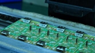
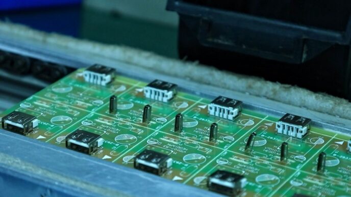
Kinex™ Bonding System For Enhanced Performance
Think of this as a super precise way to stack chips, called die-to-wafer hybrid bonding. The Kinex™ system is the first of its kind to do this all in one go. It means we can connect chips more directly, which makes them faster and more energy efficient. This is a big deal for both the brains of AI systems (logic chips) and the memory that stores all that data.
Xtera™ System For Next-Generation Transistors
We’re talking about the tiny switches inside chips, called transistors. The latest ones, like Gate-All-Around (GAA) transistors, are key for making AI chips faster. The Xtera™ system is designed to build these transistors perfectly. It lays down these special material layers, called epitaxial layers, without any gaps or flaws. This is super important for getting the best performance out of transistors, especially as we push towards 2-nanometer sizes and beyond.
Here’s a quick look at what the Xtera system tackles:
- Void-Free Structures: It stops little air bubbles from forming inside the transistor’s source and drain areas, which can mess with performance.
- Uniform Growth: It makes sure the material grows evenly across the entire chip, so all the billions of transistors work the same.
- Efficiency: It uses less gas during the process, which is good for the environment and costs.
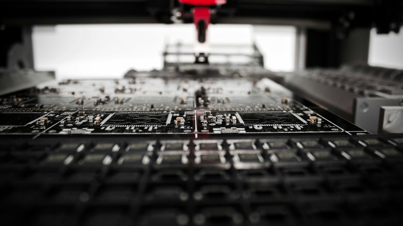
PROVision™ 10 For Complex 3D Chip Yield
Chips today aren’t flat anymore; they’re built in layers, like a tiny skyscraper. Figuring out if these complex 3D structures are built correctly is tough. The PROVision™ 10 system uses a special kind of electron beam (eBeam) to see what’s going on inside these chips with incredible detail. It can even see through multiple layers to check for problems.
Key features of the PROVision 10 include:
- Sub-Nanometer Resolution: It can spot defects that are smaller than a nanometer, which is unbelievably tiny.
- Deep Imaging: It can look deep into the 3D structures, not just the surface.
- Speed: It checks chips fast enough to keep up with production lines, helping to catch problems early and improve the number of good chips made (yield).
Breakthroughs In Materials Engineering
Making chips smaller and faster means we have to get really good at working with materials at a tiny, tiny level. It’s not just about shrinking things down anymore; it’s about building them in new ways to get the best performance.
Enabling Gate-All-Around Transistors At 2nm
Gate-All-Around (GAA) transistors are the next big thing for making chips more powerful. The tricky part is building the source and drain areas, which are like the on-off switches for the transistor. We use a process called epitaxy, or ‘epi’, to grow these materials precisely. But filling the super deep and narrow trenches needed for GAA transistors without any gaps or flaws is tough. If there are voids or the material isn’t grown evenly, the transistor won’t work as well and might fail sooner.
Applied Materials has a new system, the Centura™ Xtera™ Epi system, designed to tackle this. It uses a special chamber that’s smaller and has built-in cleaning steps. This helps grow the materials perfectly, filling those tricky trenches without any voids. It’s also more efficient with gases, using less than half of what older methods needed. Plus, it keeps an eye on the growth process, adjusting it as the material builds up. This means the layers are more uniform across the entire chip, improving how consistent the billions of transistors are with each other by over 40 percent.
Optimizing High-Bandwidth Memory Integration
High-Bandwidth Memory (HBM) is super important for AI and graphics processing because it allows for much faster data access. Integrating HBM with the main processor chip is key to boosting overall system performance. This often involves stacking multiple memory chips on top of each other or directly onto the processor. The challenge here is making sure all these connections are solid and reliable, especially as we try to pack more and more into a smaller space. We need to make sure the signals can get where they need to go quickly and without errors. This means the materials used for connecting these stacked chips have to be just right – strong, conductive, and perfectly aligned.
Innovations In Advanced Packaging Solutions
As chips get more complex, how we put them together, or ‘package’ them, becomes just as important as the chips themselves. Advanced packaging lets us combine different types of chips, like processors and memory, into a single unit. This can make devices faster and more power-efficient. Think of it like building a custom sports car instead of just upgrading a regular sedan. We’re looking at new ways to stack chips, connect them, and manage heat. This includes things like 3D stacking, where chips are piled on top of each other, and hybrid bonding, which creates super-tight connections between chips. The goal is to create systems that are not only powerful but also smaller and use less energy, which is a big deal for everything from smartphones to massive data centers.
Revolutionary Metrology For Future Chips
As chips get smaller and more complicated, figuring out if they’re made right becomes a huge challenge. Traditional methods just can’t keep up anymore. That’s where new metrology systems come in, like Applied Materials’ PROVision™ 10. This isn’t your grandpa’s microscope; it uses electron beam (eBeam) technology to see things on a scale we couldn’t before.
Sub-Nanometer Resolution With Cold Field Emission
The PROVision™ 10 system is pretty special because it’s the first one out there to use cold field emission (CFE) technology. Think of it like upgrading from a blurry old TV to a super sharp 4K screen. This CFE tech lets the system see details with up to 50% better resolution than older systems. It also works way faster, up to 10 times quicker. This means we can get a much clearer picture of what’s happening at the nanometer level, which is pretty much everything in modern chip making.
Deep Imaging Capabilities For 3D Architectures
Chips aren’t flat anymore; they’re built up in layers, like a tiny skyscraper. This makes it tough to check everything. The PROVision™ 10 can actually see through these multiple layers. It creates a combined image, letting engineers check things like how different layers line up (overlay) or measure tiny features (critical dimension) that optical tools just can’t see. This is a big deal for new designs like Gate-All-Around transistors and stacked memory.
Accelerating Yield For Complex Designs
What does all this mean for making chips? It means catching problems earlier and faster. The PROVision™ 10 can spot issues like tiny voids in epitaxial layers or check the alignment between EUV layers with much more accuracy. This helps chipmakers fix problems quickly, which speeds up the whole manufacturing process and makes sure more good chips come off the line. It’s all about getting those complex, next-gen chips made reliably.
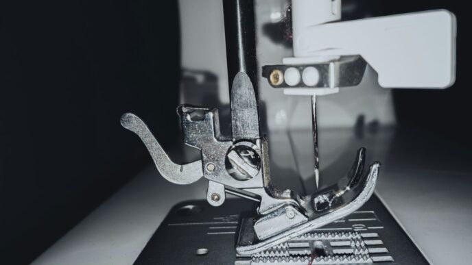
Hybrid Bonding For Superior Chip Stacking
So, stacking chips on top of each other to make them faster and use less power? It’s a big deal these days, especially for things like AI. One way to do this is called hybrid bonding. Basically, it’s a way to connect copper directly to copper between different chips or pieces of chips. This makes the connections super small and really efficient.
Integrated Die-To-Wafer Solutions
Putting chips together used to be a bit of a piecemeal process. You’d have separate machines for different steps, and that could lead to problems. Now, companies are working on systems that do more in one go. Take the Kinex™ Bonding System, for example. It’s the first system that combines putting individual chip pieces (dies) onto a whole silicon disc (wafer) with the actual bonding process. This integration means better control over where each piece goes and how it’s connected. It helps manage those really complicated multi-chip packages that are becoming common.
Achieving Smaller Interconnect Pitches
When you want to pack more into a smaller space, you need smaller connections between the parts. Hybrid bonding is great for this because it can create these tiny links. The Kinex system, with its precise placement and clean environment, is designed to make these connections even smaller. We’re talking about pitches that were hard to imagine just a few years ago. This is key for squeezing more performance out of the same area.
Ensuring Bonding Consistency And Quality
Making sure every single connection is perfect is tough. If you have a gap or a bad bond, the whole chip might not work right. The Kinex system helps here by controlling the time between different steps in the bonding process. It also has built-in checks to spot any issues early. This means you get more reliable connections, chip after chip, which is a big win for making lots of these advanced chips without too many duds.
Epitaxial Processes For Enhanced Transistor Performance
Void-Free Source-Drain Structures
Getting the source and drain parts of transistors just right is a big deal for how well they work. These areas form the channel where the magic happens. We use a process called epitaxy, or ‘epi’, to carefully put materials into deep trenches. It’s like building tiny, precise structures inside the chip. The tricky part is when these trenches get really deep and narrow, like in the new Gate-All-Around (GAA) transistors. If the epi process isn’t perfect, you can end up with gaps, or ‘voids’, and the material doesn’t grow evenly. This messes with performance and can make the chip less reliable. Applied Materials has a new system, the Centura™ Xtera™ Epi system, that’s designed to fix this. It uses a special chamber that’s smaller and has built-in cleaning steps. This helps create those void-free source-drain areas without all the usual fuss. It even uses less gas, which is good for the environment and saves money.
Optimizing Epi Growth In High Aspect Ratio Trenches
So, those super-tall, skinny trenches in modern transistors? They’re a headache for material growth. The Xtera system tackles this head-on. It has a clever way of working where it constantly adjusts the trench opening as the material is being deposited. Think of it like a sculptor carefully shaping the material as it goes down. This continuous adjustment helps the epi grow smoothly and evenly, even in those tough, high-aspect-ratio spots. This means you get better uniformity across all the billions of transistors on a chip. We’re seeing improvements of over 40 percent in how consistent the growth is from one transistor to the next. This level of control is pretty important for making sure every part of the chip performs as expected.
Improving Cell-To-Cell Uniformity
When you’re making chips with billions of tiny parts, consistency is key. If one transistor is a little different from its neighbor, it can cause all sorts of problems. The Xtera system’s ability to optimize epi growth in those challenging trenches directly leads to better cell-to-cell uniformity. This means that each individual transistor on the wafer behaves more like the others. This uniformity is what allows chipmakers to push the limits of performance and power efficiency, especially for demanding applications like AI. It’s not just about making the transistors work; it’s about making them all work together reliably and predictably. This focus on uniformity is a big step forward for next-generation chip designs.
Applied Materials Today: Driving Innovation
It’s pretty wild how fast things are moving in the chip world, right? Every year, it feels like we’re seeing new tech that just blows the last year’s out of the water. Applied Materials is right there in the thick of it, working on the materials that make all these crazy advancements possible. They’re not just making parts; they’re really pushing the science behind how chips are built.
Collaboration For Accelerated Roadmaps
One of the big things they’re doing is working super closely with chipmakers. It’s not like they just build something and hope it works. They’re getting involved way earlier in the design process. Think of it like building a custom car – you don’t just slap parts together; you plan it out from the ground up. This way, they can figure out the best materials and processes to meet specific goals, like making chips faster or use less power. It helps everyone get their next big idea out the door quicker.
Pushing The Boundaries Of Science And Engineering
Honestly, some of the stuff they’re working on sounds like science fiction. They’re dealing with materials at an atomic level, trying to get things to line up just right. For example, getting transistors to work perfectly at the 2-nanometer scale is a huge challenge. It requires totally new ways of depositing materials, making sure there are no tiny gaps or imperfections that could mess things up. They’re basically inventing new ways to build things that we didn’t even think were possible a few years ago.
Delivering Material Innovation For A Changing World
All these new chips are needed for things like AI, better graphics, and all sorts of smart devices. But making them requires a whole new set of tools and materials. Applied Materials is focused on creating these new material solutions. It’s about making sure that as technology demands more, the materials science can keep up. They’re looking at everything from how to stack chips more efficiently to how to make the tiny wires inside them work better. It’s a constant cycle of invention to keep up with what the world needs.
Looking Ahead
So, what does all this mean for the future of tech? Basically, Applied Materials is pushing hard to make the chips that power everything from AI to your phone even better. They’ve rolled out some pretty neat new gear, like the Kinex system for stacking chips and the Xtera system for building faster transistors. Plus, their PROVision 10 tool helps catch tiny flaws in these super complex chips. It’s clear they’re working on solutions for the next wave of computing, aiming for chips that are not only faster but also use less power. It’s a big deal for keeping up with the demand for smarter, more capable devices.