Applied Materials In Semiconductor Manufacturing
Applied Materials has been a major player in the semiconductor equipment scene for a long time. They really got things moving back in the day, especially with their work on cluster tools. Before these came along, processing wafers was a bit more of a free-for-all, often done in batches. But Applied Materials changed that.
Pioneering Cluster Tool Technology
Think about how things used to be done. Wafers were often processed in big groups, all at once. This worked, but it had its downsides. If one wafer had an issue, it could mess up the whole batch. Plus, keeping everything consistent across dozens or hundreds of wafers was tough. Applied Materials stepped in with their Precision 5000, a real game-changer. It was one of the first practical multi-chamber tools, meaning wafers could be processed in smaller, more controlled groups, or even one at a time, within a single machine. This allowed for better isolation between steps and improved control over the process. It was a big leap from the old ways.
Evolution of Wafer Processing Equipment
Over the years, the machines that handle wafers have gotten way more sophisticated. We’ve seen a big shift from older methods to more advanced techniques. For instance, Physical Vapor Deposition (PVD) was the go-to for laying down material for a while. But then Chemical Vapor Deposition (CVD) came along and offered new possibilities. Applied Materials has been right there, developing equipment for these different methods. They also had to adapt as wafer sizes grew, moving from smaller wafers to the 200mm and then 300mm standards we see today. Each step meant new equipment designs and challenges.
Contributions to Deposition Techniques
Depositing thin films onto wafers is a huge part of making chips. Applied Materials has made significant contributions here. They’ve developed tools for various deposition methods, including CVD and PVD. These techniques are used to lay down everything from insulating layers (dielectrics) to conductive metal layers like copper and tungsten. As chip designs get more complex, with smaller features, the need for precise material deposition becomes even more critical. Companies like Applied Materials are constantly innovating to meet these demands, developing specialized processes for different materials and layer types.
Advancements in Wafer Fabrication Processes
Back in the day, a lot of chip making happened in big batches. Think of it like doing laundry – you toss a whole load in, and hope for the best. This was the norm for processes like cleaning, etching, and even oxidation. But, as chips got more complex, this batch approach started causing problems. Results weren’t always the same from one wafer to the next, and that’s a big deal when you’re making tiny, intricate circuits.
The shift to single wafer processing changed everything. Instead of processing many wafers at once, each wafer gets its own dedicated treatment. This allows for much tighter control over each step, leading to better consistency and fewer defects. It’s like doing your laundry one delicate item at a time, ensuring each piece gets exactly what it needs. This move was seen across many areas, from cleaning and ion implantation to etching and annealing.
The Shift from Batch to Single Wafer Processing
This move wasn’t just a minor tweak; it was a fundamental change in how chips were made. Before, a whole rack of wafers might go into a cleaning bath. Now, each wafer is handled individually. This individual attention means that things like temperature, chemical concentration, and exposure time can be precisely managed for every single wafer. This is super important for things like ion implantation, where even tiny variations can mess up the electrical properties of the chip.
Here’s a look at how some processes benefited:
- Cleaning: Individual cleaning ensures no part of the wafer is missed and chemicals are applied uniformly.
- Ion Implantation: Precise control over dopant placement on a wafer-by-wafer basis.
- Etching: Consistent removal of material across the entire wafer surface.
- Annealing: Uniform heat treatment to activate dopants and repair crystal damage.
Innovations in Etching and Cleaning Technologies
Etching is basically carving out patterns on the wafer, and cleaning is, well, keeping it spotless. Both are critical. Early etching methods could be a bit rough, sometimes damaging the delicate structures being formed. Innovations focused on making these processes more precise and less aggressive. Plasma etching, for instance, uses ionized gas to remove material in a highly controlled way. For cleaning, new chemical formulations and rinsing techniques were developed to remove even the smallest particles without harming the wafer surface. Think of it as going from a power wash to a gentle, targeted scrub.
The Role of Chemical Vapor Deposition (CVD)
Chemical Vapor Deposition, or CVD, is a big deal in putting down thin films of material onto the wafer. Instead of just blasting material at the wafer like in older Physical Vapor Deposition (PVD) methods, CVD uses chemical reactions. Gases are introduced into a chamber, and they react on the wafer’s surface to form a solid film. This allows for very uniform and conformal coatings, meaning the film covers even complex 3D structures evenly. Applied Materials, for example, developed cluster tools like the Producer in the late 90s. These tools grouped multiple processing chambers together, allowing for different CVD steps to happen in sequence without breaking vacuum, which was a huge step up in productivity and quality.
Materials and Chemical Innovations
Handling Hazardous Materials in Fabrication
Making chips isn’t exactly like baking cookies. A lot of the chemicals used are pretty nasty stuff, like strong acids and solvents. Companies have to be super careful about how they store and use these. It’s not just about keeping workers safe, though that’s a big part of it. They also have to make sure none of this stuff leaks out and messes up the environment. Think about it, you’ve got these super clean rooms, and then you’re bringing in all these potentially dangerous chemicals. It’s a constant balancing act. Applied Materials, like other big players, has developed specialized equipment and processes to handle these materials safely, often using closed systems to minimize exposure. It’s a behind-the-scenes kind of innovation, but really important.
Development of Low-k Materials
As chips get smaller and more crowded, the wires connecting everything inside them start to cause problems. They get too close, and the electrical signals can interfere with each other, slowing things down. To fix this, engineers started using materials with a lower dielectric constant, or ‘low-k’ materials. These act as insulators between the wires, reducing that interference. It’s kind of like putting better insulation between electrical wires in your house to prevent shorts. The challenge was finding materials that were stable enough for the manufacturing process and actually worked well. Applied Materials has been involved in developing and integrating these low-k materials into the fabrication flow, which is a big deal for making faster, more efficient chips. This shift from older materials like silicon dioxide to these advanced low-k dielectrics was a major step in keeping up with Moore’s Law.
Advancements in Barrier Layer Technology
When you’re using copper for the wires inside a chip, it’s great because it conducts electricity really well. But copper has a tendency to spread out into other parts of the chip, which can cause all sorts of problems, like short circuits. To stop this, a thin ‘barrier layer’ is put down first. This layer acts like a dam, keeping the copper in its place. Originally, materials like tantalum nitride were used. But as chips got even smaller and denser, engineers needed something better. Applied Materials, for instance, explored using cobalt as a barrier material around 2014. Cobalt can be thinner than tantalum nitride for the same protective effect, which is super important when you’re trying to cram more and more stuff onto a tiny piece of silicon. Developing these advanced barrier layers is another one of those behind-the-scenes innovations that makes modern chips possible.
The Evolution of Semiconductor Scale and Nodes
It’s pretty wild to think about how much smaller chips have gotten over the years. We’re talking about shrinking things down to the atomic level, and it’s all tied to this idea of ‘process nodes’ and Moore’s Law. Basically, Moore’s Law is this observation that the number of transistors on a chip doubles about every two years, which means they get smaller and faster. Applied Materials has been right in the middle of making this happen.
Transitioning to Larger Wafer Diameters
When chips were first being made, the silicon wafers they were built on were pretty small. Think about 2-inch wafers back in the day. As manufacturing got better, they started using bigger wafers, like 3-inch, then 4-inch, and eventually 6-inch. The big jump came with 8-inch (200mm) wafers, which really became the standard for a long time. Then, the industry moved to 12-inch (300mm) wafers. This was a huge deal because you can fit way more chips on a larger wafer, which cuts down on the cost per chip. It also meant bigger, more expensive factories, but the payoff was worth it. Applied Materials played a big part in developing the tools needed for these larger wafers, like handling systems and deposition equipment that could cover the whole surface evenly.
Understanding Process Node Evolution
This is where things get a bit confusing, and honestly, a bit like marketing. The ‘process node’ number, like 10nm or 7nm, used to refer to a specific feature size on the chip, like the gate length of a transistor. But over time, it’s become more of a marketing term. Companies started using smaller numbers to make their chips sound more advanced, even if the actual physical dimensions weren’t always that small. For example, a ’10nm’ process from one company might be similar in density to a ‘7nm’ process from another. It’s like they’re not measuring the same thing anymore. This shift means that just looking at the node number doesn’t tell you the whole story about how dense or powerful a chip is.
Here’s a look at how the node names have changed over time, though remember, these numbers aren’t always literal measurements anymore:
- Early Days (Micrometers):
- 1971: 10 µm
- 1977: 3 µm
- 1981: 1.5 µm
- 1984: 1 µm
- Moving to Nanometers:
- 1990: 600 nm
- 1996: 250 nm
- 2001: 130 nm
- 2005: 65 nm
- 2009: 32 nm
- 2012: 22 nm
- 2014: 14 nm
- 2016: 10 nm (marketing name)
- 2018: 7 nm (marketing name)
- 2020: 5 nm (marketing name)
- 2022: 3 nm (marketing name)
- 2025: 2 nm (projected)
The Impact of Moore’s Law on Manufacturing
Moore’s Law has been the driving force behind the semiconductor industry for decades. It pushed companies to constantly innovate, making transistors smaller, faster, and more power-efficient. For Applied Materials, this meant developing new equipment and processes to handle these shrinking dimensions. Think about lithography, deposition, and etching – all these steps had to get incredibly precise. As transistors got smaller, new challenges popped up, like quantum effects and heat management. The industry’s ability to keep pushing Moore’s Law is a testament to continuous innovation in materials science and manufacturing technology. Companies like Applied Materials had to invent new ways to deposit ultra-thin films, etch incredibly fine patterns, and inspect for defects at the atomic scale. It’s a constant race to stay ahead, and it’s what makes modern electronics possible.
Key Equipment and Process Milestones
When you think about making computer chips, it’s not just about the tiny designs. A huge part of it is the machinery and the steps involved. Applied Materials has been right in the middle of a lot of these big moments in semiconductor manufacturing.
Automated Inspection Tools for Yield Management
Finding flaws early on is super important for making sure chips work right and for not wasting materials. Back in 1984, KLA came out with the first automatic tool to check reticles and photomasks. Then, in 1985, they introduced a system that could inspect silicon wafers automatically. This was a big deal because it replaced the old way of looking at wafers under a microscope, which was slow and prone to mistakes. These inspection tools are key to figuring out why some chips don’t work (that’s called yield) and how to make more good ones.
The Precision 5000 Cluster Tool
Before the 1980s, wafer processing often happened in big batches. But this could lead to inconsistencies. Applied Materials changed the game in 1985 by developing the Precision 5000. This was one of the first practical "cluster tools," meaning it had multiple processing chambers all connected to one system. This setup allowed wafers to move between different steps without being exposed to the outside air as much, leading to better control and more reliable results. It was a significant step away from older batch methods.
Innovations in Physical Vapor Deposition (PVD)
Depositing thin films of material onto wafers is a core part of chip making. For a long time, Physical Vapor Deposition (PVD) was the main way to do this. PVD involves physically moving material from a source onto the wafer, often using a process called sputtering. While PVD is still used, the industry has seen a lot of development in deposition techniques. Applied Materials has been a major player here, offering advanced PVD systems that allow for precise control over the deposited layers. These layers are critical for the electrical properties and performance of the final chips.
Safety and Environmental Considerations
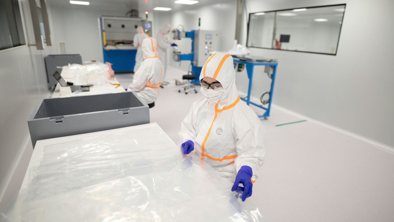
When you look inside a modern semiconductor fab, the safety and environmental systems are everywhere—sometimes obvious, sometimes hidden. They have to be: the chemicals, systems, and even the air can be dangerous if not managed carefully. Making chips is more than just high-tech wizardry; it’s about keeping people and the planet out of harm’s way. Here’s where Applied Materials’ contributions come into play.
Automated Systems for Worker Safety
Working directly with high-voltage gear and nasty chemicals isn’t part of anyone’s dream job. Automation has changed the game for worker safety in semiconductor fabs. Machines now handle the scariest jobs, reducing the risk for real people. Here’s what that looks like day-to-day:
- Wafer transport: Remote-guided robots shuttle wafers from tool to tool, so staff don’t have to enter hazardous zones.
- Chemical dosing: Precision pumps and valves dispense acids and dopants, so workers aren’t dealing with them by hand.
- Enclosed systems: Many processes take place in tightly-sealed chambers, keeping chemical vapors and dust away from people.
The result? Accidents involving direct chemical exposure are now rare.
Exhaust Management Systems in Fabrication
It’s not just what’s on the fab floor that’s dangerous; toxic fumes and waste gases are a constant concern. To tackle this, sophisticated exhaust management systems capture, scrub, or neutralize emissions before they escape into the air. Here’s how fabs handle their exhaust:
| System | What It Does | Typical Use |
|---|---|---|
| Wet Scrubbers | Dissolve acidic gases | Cleanroom venting |
| Combustors | Burn off volatile chemicals | CVD/PVD tools |
| Absorber Filters | Trap metals or solvents | General air output |
Fabs also keep close tabs on real-time gas sensors, so if a leak ever happens, alarms sound and systems shut down fast.
Addressing Environmental Impact of Manufacturing
Making chips uses huge amounts of energy and water—not exactly eco-friendly if left unchecked. But the industry’s been under pressure to cut its footprint:
- Water recycling: Factories use specialized filtration to reuse water multiple times before it’s discarded.
- Solvent recovery: Organic chemicals are captured and reprocessed for later use, cutting waste.
- Power conservation: Facilities invest in low-energy lighting, smarter cooling, and more efficient machines to reduce electricity demand.
Applied Materials and other manufacturers publish sustainability reports every year, tracking:
| Metric | 2025 Average | Trend vs. 2015 |
|---|---|---|
| Water use (m³/waf) | 1.4 | -15% |
| Energy (kWh/waf) | 8.2 | -10% |
| Chemical waste (kg/waf) | 0.52 | -18% |
With increasingly strict rules worldwide, these numbers have to keep moving downward. It’s not perfect, but it’s improving each year.
Semiconductor manufacturing pushes the limits of technology, but also safety and environmental controls. Every step forward—whether it’s a new tool, cleaner air, or less waste—makes a big difference for the people making chips and the world outside the fab walls.
Wrapping Up
So, that’s a look at how Applied Materials fits into the whole semiconductor manufacturing picture. It’s pretty wild to think about all the steps and the specialized gear needed just to make the chips that power our phones and computers. From what we’ve seen, Applied Materials plays a big part in making a lot of that happen. They’re involved in a bunch of different stages, from depositing materials to cleaning wafers. It’s a complex world, for sure, and it’s clear that companies like Applied Materials are key players in keeping things moving forward. It makes you appreciate the tech a bit more, doesn’t it?