
So, ASML has this new machine, the hyper-na euv, and it’s kind of a big deal for making computer chips. Think of it as the next level up in making things super, super small. This isn’t just a small tweak; it’s a whole new way to get more power into the tiny chips that run everything from your phone to the biggest supercomputers. It’s been a long time coming, and it’s going to change how we make electronics.
Key Takeaways
- ASML’s new hyper-na euv machines are a huge step forward, letting us make chips with features smaller than 2 nanometers, which is pretty wild.
- This technology is the result of about ten years of work and is crucial for making the next generation of powerful chips needed for AI and advanced computing.
- While these machines are incredibly advanced, they also come with a massive price tag, leading some companies to adopt them more slowly than others.
- The development and sale of hyper-na euv technology are caught up in global politics, with trade rules affecting where these machines can go.
- Investing in companies that use or make this technology could be a big gamble, but it’s also key to the future of electronics and staying competitive.
Unpacking The Hyper-NA EUV Technological Leap
The Numerical Aperture Advantage
So, what’s the big deal with this "Hyper-NA" EUV stuff? It all comes down to something called numerical aperture, or NA. Think of it like the lens on a camera – a higher NA means it can gather more light and focus it more precisely. ASML’s new machines have a much higher NA (0.55) compared to their older EUV models (0.33). This jump is a pretty big deal because it lets them print much smaller features on silicon wafers. We’re talking about features that are about 1.7 times smaller, which means you can cram nearly three times as many transistors onto a chip. This is exactly what’s needed to get us to those super-advanced sub-2 nanometer logic nodes that everyone’s talking about for the next generation of processors.
Enabling Sub-2 Nanometer Logic Nodes
Getting chips down to the sub-2 nanometer scale is incredibly tough. It’s like trying to draw incredibly fine lines with a pen that’s too thick. Older methods often required multiple passes, or "multi-patterning," to get the design just right. This adds a lot of steps, complexity, and potential for errors, which can lower the number of good chips you get from each wafer. The higher NA in these new ASML machines means they can print these tiny features in a single pass. This simplification is a game-changer for manufacturing at these advanced nodes. It means less hassle, potentially fewer defects, and a clearer path to making chips that are smaller, faster, and more power-efficient.
A Decade In The Making
This isn’t something that just popped up overnight. ASML has been working on the ideas behind High-NA EUV for about ten years. Developing the technology to create and control that super-short wavelength EUV light, and then building machines with these massive, incredibly precise optics – it’s been a huge undertaking. They had to figure out how to generate the light itself, which involves shooting tiny droplets of molten tin with lasers to create a plasma hotter than the sun, all in a vacuum because EUV light gets absorbed by pretty much everything. Then there’s the optics, made by companies like Zeiss, which are some of the flattest surfaces ever created. It’s a testament to a lot of hard work and innovation from many different companies working together.
ASML’s Hyper-NA: A Cornerstone For Advanced Chip Manufacturing
Accelerating The Race For Chip Leadership
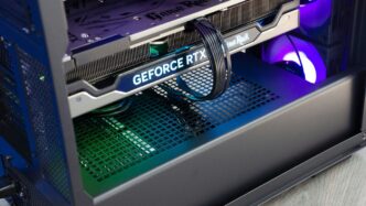
ASML’s High-NA EUV machines are basically the new gold standard for making the most advanced computer chips. Think of them as the ultimate precision tools for the job. Companies like Intel are already getting their hands on these, and it’s really speeding things up for them. This technology is what lets chipmakers create features that are smaller than 2 nanometers, which is pretty wild when you think about it. It’s like trying to draw a line thinner than a single strand of DNA. This means the chips powering our future AI, supercomputers, and even our phones will be way more powerful and efficient. It’s a big deal for any company wanting to be at the top of the chip game.
Simplifying Complex Manufacturing Processes
Making cutting-edge chips used to involve a lot of complicated steps, kind of like trying to assemble a really intricate model airplane with tiny, fiddly parts. ASML’s High-NA EUV machines help cut down on some of that complexity. By using a higher numerical aperture (that’s the 0.55 NA, a big jump from the older 0.33 NA), these machines can print finer details in fewer steps. This means fewer chances for things to go wrong, which is always good. It’s a bit like having a super-precise stencil that lets you get the job done right the first time, more often.
Unlocking Unprecedented Transistor Densities
So, what does all this precision actually mean for the chips themselves? It means you can pack way more transistors onto a single piece of silicon. Imagine trying to fit more and more tiny Lego bricks into the same small box. With High-NA EUV, chipmakers can achieve a nearly threefold increase in transistor density compared to older EUV systems. This is how we get to those sub-2 nanometer logic nodes and advanced memory chips. It’s the key to making chips smaller, faster, and more energy-efficient, which is exactly what we need for all the new tech coming our way.
The Road Ahead: Navigating The Hyper-NA Horizon
So, what’s next for this super-precise chip-making tech? It’s not like ASML just flips a switch and everything is suddenly easier. There’s a whole lot of work still to do, both in the immediate future and looking way down the line.
Short-Term Integration And Optimization
Right now, the big focus is getting these new High-NA machines up and running smoothly. Think of it like getting a brand-new, super-complicated piece of equipment for a factory. The first few years are all about figuring out the kinks, making sure it works reliably, and training people to use it properly. Companies like Intel are really pushing to show what this tech can do for their next-generation chips, aiming for nodes like 18A and 14A. ASML is planning to ship a handful of these machines in 2025, and they expect sales to really take off. Other big players, like TSMC and Samsung, are also doing their homework, with limited production runs expected around 2026 or 2027. The main challenge here is for chip designers to actually change how they design chips to take full advantage of what High-NA offers, like cutting down on extra manufacturing steps.
Long-Term Scaling Beyond 2 Nanometers
Looking further out, say three to five years from now, High-NA EUV is supposed to be the main tool for making chips smaller than 2 nanometers. We’re talking about aiming for 1.5nm and even smaller. ASML figures that mass production using this tech will really kick off after 2027. This is going to be super important for keeping up with the massive demand for chips used in AI and high-performance computing. It’s a relentless push for smaller and smaller transistors.
The Pursuit Of Hyper-NA And Beyond
But ASML isn’t stopping with just High-NA. They’re already talking about "Hyper-NA" EUV, which would have an even higher numerical aperture, maybe around 0.75. This could be ready for use sometime between 2030 and 2035. It shows that the drive to shrink things down just keeps going, even though it gets harder and harder. It’s a bit like trying to run faster and faster – eventually, you hit a wall, but you keep trying to find a way over it. Some memory chip makers, though, might not adopt High-NA as quickly because of the high costs and because newer memory designs might not need it as much. Plus, there’s always the possibility that other manufacturing techniques, like advanced etching, could become more important for certain types of chips.
Global Impact And Geopolitical Currents
Navigating Tariff Implications
The introduction of ASML’s Hyper-NA EUV technology isn’t just a technical leap; it’s also a major player in global trade and politics. Because these machines are so specialized and expensive, only a few countries and companies can really afford them. This creates a situation where access to this cutting-edge tech can become a point of negotiation, or even a tool, in international relations. Tariffs and trade restrictions, especially those aimed at limiting the spread of advanced semiconductor manufacturing capabilities, can significantly alter the cost and availability of these critical tools. For instance, export controls can force countries to seek alternative, potentially less advanced, solutions or invest heavily in developing their own domestic capabilities, which is a long and difficult road. This dynamic directly impacts the global supply chain, making it more complex and potentially less stable for everyone involved.
Shaping Global Power Balances
Semiconductor manufacturing is already a huge part of global power, and Hyper-NA EUV just cranks that up a notch. Countries that can produce the most advanced chips, using machines like ASML’s, gain a significant economic and strategic advantage. Think about it: AI, advanced computing, and next-gen defense systems all rely on these tiny, powerful chips. So, whoever controls the most advanced chip-making technology, or has the best access to it, has a serious edge. This technology is at the heart of competition between major global players, influencing everything from economic growth to national security. It’s not just about making better phones; it’s about who leads in the technologies that will define the future. ASML’s position, as the sole provider of these advanced lithography systems, puts it right in the middle of these global discussions about technological leadership and supply chain security.
Bolstering Domestic Manufacturing
With the global landscape shifting, many nations are looking inward, trying to build up their own semiconductor manufacturing capabilities. The reliance on a single company like ASML for the most advanced tools highlights the vulnerability of global supply chains. Governments are therefore pushing initiatives to encourage domestic production, offering incentives and funding to companies that can bring advanced chipmaking, or at least key parts of the supply chain, back home. This isn’t just about economic independence; it’s also about ensuring access to critical technologies during times of geopolitical tension. The goal is to reduce dependence on foreign suppliers and create more resilient domestic industries. This push for self-sufficiency, while challenging, is a direct response to the realities presented by technologies like Hyper-NA EUV and the global dynamics surrounding them.
The Hyper-NA Investment Landscape
So, let’s talk about the money side of things with this new Hyper-NA EUV tech. It’s a pretty big deal, and naturally, it’s got investors looking closely. We’re talking about some serious cash being poured into this, and it’s not exactly a small bet. The sheer cost of these machines means only the biggest players can even consider them right now.
A Risky But Rewarding Investment
Buying into ASML’s Hyper-NA EUV is definitely a high-stakes game. These lithography machines cost hundreds of millions of dollars each. Think about it – that’s a massive upfront cost for any chip manufacturer. Intel, for example, is jumping in early, but others like TSMC and Samsung are taking a more measured approach, probably due to the price tag and the need to figure out how best to use them. It’s a bit like buying the most advanced, expensive tool for a workshop; you better be sure you can use it to make something really valuable.
Driving Down Chip Production Costs
While the initial investment is huge, the idea is that in the long run, Hyper-NA EUV will actually make producing super-advanced chips cheaper. How? By simplifying the manufacturing process. Right now, making the tiniest transistors often involves multiple steps, like printing the same pattern over and over. Hyper-NA EUV can print finer details in fewer steps. This means fewer wafers wasted, less time spent on each chip, and ultimately, a lower cost per chip once everything is dialed in. It’s a bit of a paradox, but spending a fortune now could save fortunes later.
Key Indicators For Investors
If you’re thinking about investing in this space, there are a few things to keep an eye on. First, watch how many of these Hyper-NA machines ASML actually sells and ships. Are more companies besides Intel signing up? Second, listen to what the big chipmakers are saying about their plans. Are they sticking to their timelines for using this tech, or are they changing their minds because of the cost or other issues? ASML’s financial reports, especially their outlook for the next year, will be super important. Also, keep an eye on global politics, particularly anything affecting trade with China, as that can really shake things up. Finally, don’t forget to look at how well ASML’s stock is doing; ASML’s stock has experienced its most significant decline recently, which tells you the market is paying attention to these factors.
Wider Significance: A New Era Of Innovation
The Indispensable Enabler For AI And HPC
So, ASML’s new Hyper-NA EUV machines. They’re not just another piece of fancy equipment; they’re pretty much the only way forward for making the super-advanced chips that power things like AI and high-performance computing. Think about it – these new machines let us shrink components down to sizes we’ve only dreamed of, like below 2 nanometers. This is exactly what’s needed for the massive data crunching and complex calculations that AI and HPC demand. Without this tech, we’d hit a wall pretty quickly.
Phased Adoption And Ecosystem Adaptations
Getting this Hyper-NA tech up and running isn’t like flipping a switch. It’s a big, complex process. Companies are adopting it in stages. Right now, in late 2025, it’s mostly in research and development. We’re expecting to see some limited production starting around 2026 or 2027. This phased approach makes sense because the machines are incredibly expensive and require significant changes to existing manufacturing facilities. It’s not just about the lithography machine itself; it’s about the whole chain of suppliers and partners – from the optics makers to the companies that clean the wafers. Everyone has to be ready and working together.
Ensuring Continued Progression Of Moore’s Law
For decades, Moore’s Law has been the guiding principle in chip making, saying we can roughly double the number of transistors on a chip every couple of years. It’s what’s given us faster phones, better computers, and all sorts of tech advancements. Hyper-NA EUV is the key to keeping that going. It allows for much finer detail in chip designs, meaning more transistors can be packed into the same space, or even smaller spaces. This means chips will continue to get more powerful and efficient, which is pretty important if we want to keep seeing new innovations in areas like AI, virtual reality, and beyond. It’s the next big step in that long journey of making electronics smaller and better.
The Road Ahead
So, what does all this mean for the future? ASML’s High-NA EUV machines are a pretty big deal, no doubt about it. They’re letting us make chips smaller and better than ever before, which is exactly what we need for things like AI and super-fast computers. It’s not going to be a simple path, though. These machines cost a fortune, and getting them to work perfectly takes time and a lot of know-how. Plus, there are all sorts of global politics involved that can make things tricky. But even with the challenges, ASML is already thinking about what’s next, hinting at even more advanced machines down the line. It really feels like we’re at the start of something new in how we build the tech that runs our world.
Frequently Asked Questions
What is ASML’s Hyper-NA EUV technology?
Think of ASML’s Hyper-NA EUV as a super-powered magnifying glass for making computer chips. It uses a special kind of light (Extreme Ultraviolet) and a very precise lens system (the ‘NA’ part, which stands for Numerical Aperture) to draw incredibly tiny details onto silicon wafers. ‘Hyper-NA’ means it has an even better, more powerful lens than previous versions, allowing it to draw even smaller and more complex patterns.
Why is this Hyper-NA technology so important for making chips?
This new technology is like a shortcut to making much smaller and more powerful chips. Before, making tiny parts of a chip required many complicated steps. Hyper-NA lets chipmakers draw these tiny parts in fewer steps, which means they can pack more computer power into the same space. This is super important for things like faster phones, smarter computers, and better artificial intelligence.
How long did it take ASML to create this Hyper-NA technology?
Creating this advanced chipmaking machine wasn’t a quick job. ASML spent about ten years working on it, refining the ideas and building the complex machinery. It’s a bit like building a super-advanced race car – it takes a lot of time, effort, and smart engineering to get it just right.
Are these Hyper-NA machines very expensive?
Yes, these machines are incredibly expensive, costing hundreds of millions of dollars each! Because they are so costly and complex, only a few big chip companies can afford to buy and use them right now. This means not everyone can use this cutting-edge technology immediately.
Who is using this new Hyper-NA technology?
Some of the biggest chip companies in the world, like Intel, are starting to use these machines. They are using them to build the next generation of super-advanced computer chips. Other major players like TSMC and Samsung are also looking at how and when they will use this technology.
What does the future look like with Hyper-NA?
Hyper-NA is paving the way for chips that are smaller than 2 nanometers, which is incredibly tiny! This will lead to even more powerful devices for AI, gaming, and scientific research. ASML is already thinking about even more advanced versions, so the race to make smaller and better chips is definitely continuing.