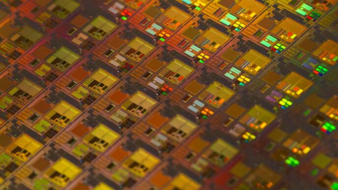
So, you’ve heard about microchips, right? They’re the brains of pretty much everything we use these days. But those tiny silicon bits can’t just float around on a circuit board. They need a protective shell, a way to connect to everything else, and a way to not overheat. That’s where IC packaging comes in. It’s like the housing for your phone or the case for your computer – it does a lot more than just look pretty. We’re going to break down what IC packaging is all about, look at the different kinds out there, and see where this whole field is headed.
Key Takeaways
- IC packaging is basically the protective case and connector for tiny computer chips, keeping them safe and letting them talk to the rest of the electronics.
- Older, but still around, types of IC packages include DIP, SOP, and QFP, each with its own pros and cons for different uses.
- Newer, more advanced IC packaging like BGA and CSP packs more connections into smaller spaces and often handles heat better.
- The latest trends are pushing towards even smaller, more integrated solutions like System-in-Package (SiP) and 3D ICs, plus new ways to build packages right on the wafer.
- Picking the right IC package means thinking about how well it works, how much it costs, how easy it is to make, and what the final product needs to do.
Understanding The Fundamentals Of IC Packaging
What Are IC Packages?
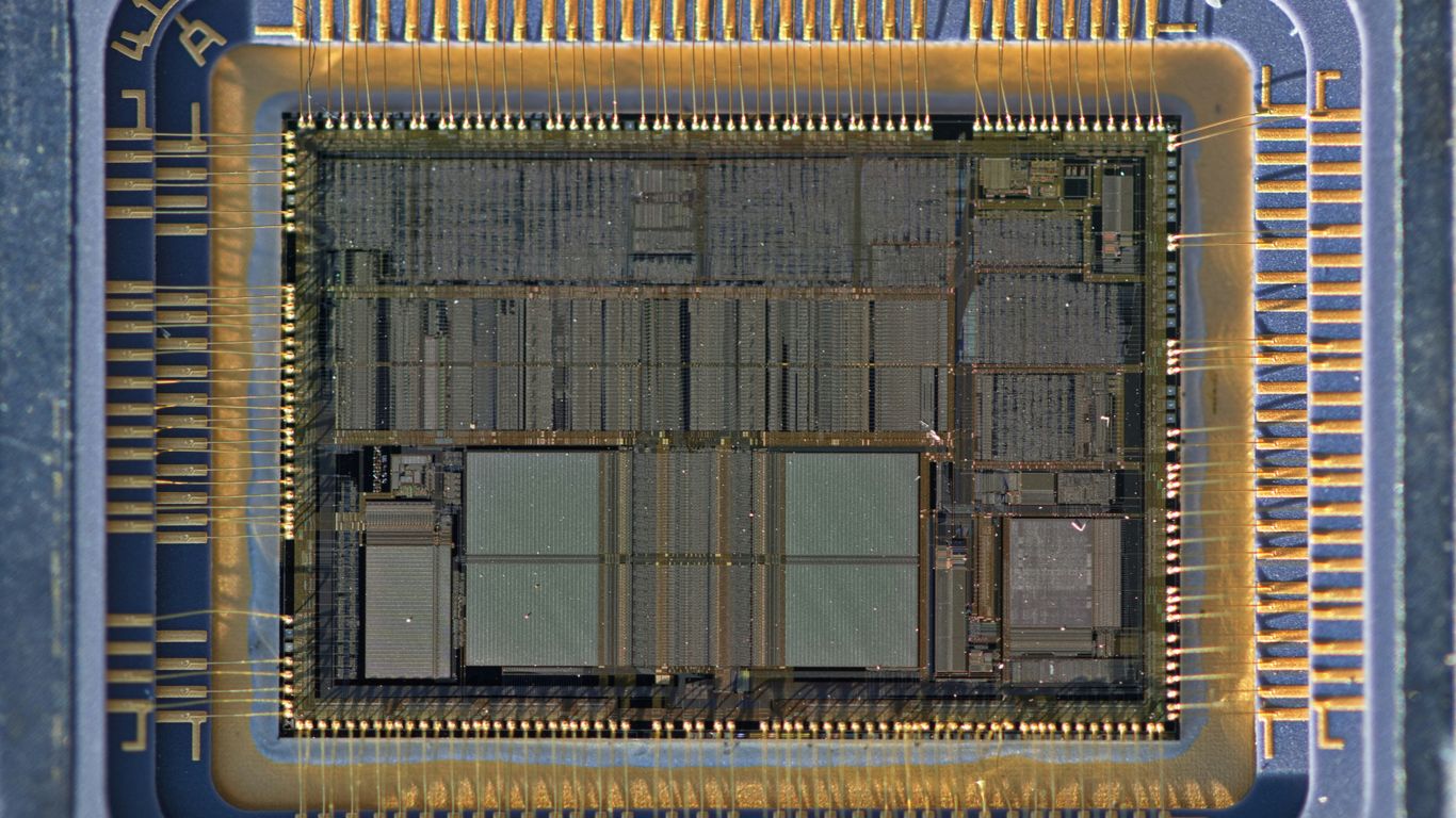
So, you’ve got these tiny, super-complex silicon chips, right? They’re the brains of our gadgets, but they’re also pretty delicate. An IC package is basically the protective shell and the connection point for these chips. Think of it like the case for your phone – it keeps the important stuff inside safe and lets you interact with it. It’s not just a simple box; it’s engineered to shield the chip from things like moisture, dust, and accidental bumps, while also making sure it can talk to the rest of the electronic system it’s part of. Without these packages, our electronics would fall apart pretty quickly.
Why IC Packaging Matters In Modern Electronics
It might seem like just a small detail, but the packaging of an integrated circuit (IC) is a really big deal in how our electronics actually work. It’s the bridge between the microscopic world of the silicon chip and the macroscopic world of our devices. A good package means the chip stays protected from the environment – no water damage or dust bunnies getting inside. It also provides the pins or connections that allow the chip to receive power and send out signals to other parts of the circuit board. Plus, and this is super important, it helps manage the heat that these chips generate. If a chip gets too hot, it can slow down or even break. So, the right packaging is key for reliability, performance, and making sure your phone or computer doesn’t overheat.
Key Functions Of IC Packaging
IC packages do a few main jobs, and they’re all pretty important:
- Protection: This is the most obvious one. The package acts as a shield, keeping the sensitive silicon die safe from physical damage, moisture, and contaminants. It’s like a suit of armor for the chip.
- Electrical Connection: The package provides the pathways, usually in the form of pins, balls, or pads, that connect the chip to the printed circuit board (PCB). This allows the chip to communicate with other components and receive power.
- Thermal Management: Chips generate heat when they’re working hard. The package helps to spread out and dissipate this heat, preventing the chip from overheating and ensuring it operates within its designed temperature limits.
- Mechanical Support: It gives the delicate silicon die something solid to be attached to, making it easier to handle during manufacturing and assembly processes.
- Form Factor: Packages also help define the physical size and shape of the component, which is important for fitting everything into compact devices like smartphones or wearables.
Exploring Traditional IC Package Types
Alright, let’s talk about the old-school ways of housing our integrated circuits. Before we got into all the fancy, super-small stuff, there were some workhorses that really got the job done. These traditional packages are still around, especially when cost or ease of use is a big deal.
Dual Inline Packages (DIP)
Think of DIPs as the classic "brick" of the IC world. They’ve got these two rows of pins sticking out, one on each side. You’d literally push these pins through holes in a circuit board and then solder them in place. They’re pretty robust and easy to handle, which made them super popular for a long time, especially for hobbyists and in educational kits. You’ll still find them in older equipment or simpler devices where you don’t need a ton of connections or super-high speeds.
- Easy to work with: Great for breadboarding and manual assembly.
- Durable: The through-hole design offers good mechanical strength.
- Cost-effective: Generally cheaper to produce than newer types.
Small Outline Packages (SOP)
As electronics started getting smaller, the DIP was a bit too bulky. That’s where the SOP came in. These are designed for surface mounting, meaning they sit on top of the circuit board and get soldered directly to pads, no holes needed. They’re smaller than DIPs and have leads that kind of "wing out" from the sides. They offered a good balance between size and the number of connections you could get, making them a go-to for a lot of consumer electronics.
Quad Flat Packages (QFP)
Now, if you needed even more connections and a relatively slim profile, the QFP was a popular choice. Imagine an SOP, but with leads coming out from all four sides of the chip. This design allows for a much higher pin count, which is great for more complex chips like microprocessors. The "gull-wing" shape of the leads helps with soldering and makes them a bit more reliable. They were a big step up for packing more power into smaller spaces, and you’d find them in everything from computers to industrial controls.
Advanced IC Packaging Solutions
As electronics get smaller and more powerful, the way we package our chips has to keep up. We’re moving beyond the simpler designs of the past into some really interesting territory. These advanced solutions are all about packing more functionality into smaller spaces, and doing it more efficiently.
Ball Grid Array (BGA) And Land Grid Array (LGA)
Think of BGAs and LGAs as the next step up from those older quad flat packages (QFPs). Instead of pins sticking out the sides, BGAs use little solder balls on the bottom of the package. This means way more connections can be made, and they’re spread out over the whole underside of the chip. This is great for performance because the connections are shorter, and it also helps with heat dissipation. LGAs are similar, but instead of balls, they have little pads that press down onto a socket. This makes them really easy to swap out, which is handy for things like CPUs in computers.
- BGAs are fantastic for high-pin-count applications where good electrical performance is a must.
- LGAs are often used where serviceability or easy replacement is a priority.
- Both offer better thermal management compared to older pin-based packages.
Chip-Scale Packages (CSP)
CSPS are pretty much as small as you can get, with the package size being only slightly larger than the actual silicon die itself. It’s like the package is almost the same size as the chip inside. This is a huge win for miniaturization, making devices like smartphones and wearables much thinner and lighter. They use tiny solder balls or bumps directly on the die’s surface for connections. The main idea here is to get the chip as close to its final application as possible, minimizing space and signal path.
Flip-Chip Technology
Flip-chip is a way to connect the silicon die directly to the substrate or circuit board. Instead of wire bonding from the edges of the chip, the die is flipped upside down, and solder bumps on its surface connect directly to the board. This is a big deal because it allows for a much higher density of connections and significantly shorter signal paths. It’s especially useful for high-performance chips like processors and graphics cards where speed and bandwidth are critical. It also helps with thermal management because the heat can be drawn away more directly from the die.
Next-Generation IC Packaging Technologies
Okay, so we’ve talked about the older ways of packaging chips. Now, let’s get into the really cool stuff – the next-generation technologies that are making our gadgets smaller, faster, and way more powerful. It’s like packing more and more into less and less space, which is pretty wild when you think about it.
System-in-Package (SiP)
Think of SiP as a "system on a chip," but instead of cramming everything onto one piece of silicon, you’re putting multiple chips and other bits and pieces into a single package. It’s like a mini-assembly of specialized components working together. This is super handy for devices where space is really tight, like smartwatches or those little IoT sensors you see everywhere. It cuts down on the board space needed and can actually make the whole thing work better.
3D IC Packaging Techniques
This is where things get stacked, literally. Instead of laying chips out flat, 3D IC packaging stacks them on top of each other. They’re connected using tiny vertical pathways called through-silicon vias (TSVs). This vertical stacking really boosts how much you can fit into a small area. It’s great for things that need a lot of processing power in a small package, like advanced computer chips or memory modules. Plus, it can make them more power-efficient.
Wafer-Level and Fan-Out Packaging
These techniques take the packaging process right down to the wafer level, before the individual chips are even cut apart. Wafer-level chip-scale packaging (WLCSP) makes the package almost the same size as the chip itself. Fan-out wafer-level packaging (FOWLP) is a bit different; it actually expands the chip’s connections outwards on a special layer. This lets you add more connections without making the chip itself bigger, which is a clever trick. It’s becoming common in things like mobile processors and advanced sensors because it helps with both performance and keeping power use down.
Selecting The Optimal IC Package
So, you’ve got your shiny new integrated circuit, but how do you actually connect it to the rest of your electronic creation? That’s where the IC package comes in. Picking the right one isn’t just about looks; it’s a pretty big deal that can affect how well your gadget works, how long it lasts, and even how much it costs to make. It’s like choosing the right shoes for a marathon – you wouldn’t wear flip-flops, right?
Key Considerations For IC Package Selection
When you’re staring down a pile of different package options, it can feel a bit overwhelming. But don’t sweat it! There are a few main things to keep in mind. Think of it as a checklist to make sure you’re not missing anything important.
- Performance Needs: What does this chip actually do? If it’s a powerhouse processor crunching numbers at lightning speed, it’s going to need a package that can handle the heat and send signals super fast. Simpler chips might be fine with less fancy options.
- Size Matters: How big or small does your final product need to be? If you’re building something tiny like a smartwatch, you’ll need a compact package. For larger devices, you might have more wiggle room.
- Heat Management: Some chips get really hot when they’re working hard. The package needs to help get that heat away, otherwise, things can go wrong. Packages with good thermal performance are key for these hot-running components.
- Cost: Let’s be real, budget is always a factor. Some packages are cheaper to make and assemble than others. You’ll need to find that sweet spot between getting the performance you need and not breaking the bank.
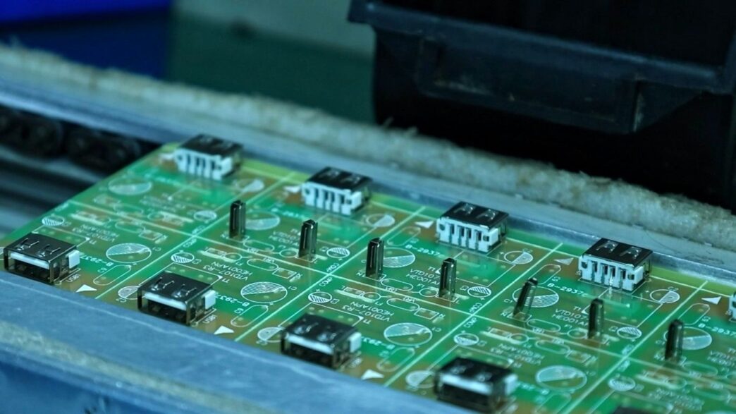
- How It Connects: Think about how the package will attach to your circuit board. Some use little pins that go through holes, while others have tiny balls or pads that sit on the surface. This affects how easy it is to assemble and how reliable the connection is. For many small electronic products, Surface Mount Technology (SMT) is a popular choice.
Application-Specific Guidance For IC Packages
Different jobs call for different tools, and the same goes for IC packages. What works great for a smartphone might be overkill for a simple thermostat.
- Consumer Electronics: Think smartphones, laptops, and smart home devices. These often need small, lightweight packages that can handle decent performance. Chip-Scale Packages (CSP) and Ball Grid Arrays (BGA) are common here because they pack a lot of connections into a small space.
- Automotive: Cars have a lot of electronics, and they need to be tough. Packages used here need to handle temperature swings and vibrations. Reliability is super important, so you might see robust packages that can withstand harsh conditions.
- Industrial Equipment: Think factory automation or heavy machinery. These applications often prioritize durability and long-term reliability. Sometimes, simpler, more robust packages are preferred, especially if cost is a major driver and extreme miniaturization isn’t the top priority.
- High-Performance Computing: For things like servers, supercomputers, or advanced graphics cards, raw speed and massive data handling are the name of the game. Packages like BGAs and Flip-Chip technologies are often used because they offer excellent electrical performance and thermal management for these demanding chips.
Balancing Performance, Cost, and Manufacturability
Ultimately, choosing an IC package is all about finding the right balance. You can’t always have the absolute best performance and the lowest cost and the easiest manufacturing all at once. It’s a juggling act.
| Requirement | Example Package Types | Notes |
|---|---|---|
| Smallest Size | CSP, WLCSP | Ideal for wearables and mobile devices. |
| High Pin Count | BGA, QFP | Good for complex processors and FPGAs. |
| Best Thermal | Flip-Chip, BGA | For high-power chips that generate a lot of heat. |
| Lowest Cost | DIP, SOP | Often used in simpler, cost-sensitive applications. |
| Ruggedness | Through-hole packages (like DIP) | Offers strong mechanical connection, good for harsh environments. |
The goal is to select a package that meets your application’s core needs without overspending or creating manufacturing headaches. Sometimes, a slightly less performant but much cheaper and easier-to-assemble package is the smarter choice for your project. It’s a decision that requires looking at the whole picture, not just one piece.
Emerging Trends In IC Packaging
Advanced Manufacturing Processes
The world of electronics is always moving faster, and the way we package chips has to keep up. We’re seeing some really cool new ways to put these tiny components together. Think about additive manufacturing, which is basically 3D printing for IC packages. It lets engineers quickly make prototypes, cutting down the time and cost of getting new designs out there. Then there’s laser-assisted bonding. This is super precise, helping connect really dense circuits, which is a big deal for those super small packages like CSPs and flip-chips. It’s all about making things smaller and faster, you know?
Innovations In Materials For IC Packaging
It’s not just about how we put the chips together, but also what we use to build the packages. Heat is a big problem for powerful chips, so researchers are looking at new materials to help get rid of it. Things like graphene and carbon nanotubes are being explored for thermal interface materials. They’re way better at moving heat away than what we’ve used before. For high-speed stuff, like for 5G and beyond, we need materials that don’t mess with the signals. So, low-dielectric materials are becoming really important. And get this – there’s even work being done on biodegradable materials. The idea is to make packaging that’s kinder to the planet, reducing electronic waste down the line. It’s a pretty big shift in thinking.
The Role Of Automation And AI In Packaging
Putting all these advanced packages together isn’t simple, and that’s where automation and artificial intelligence come in. Machine learning and AI tools are being used to help design the packages and even manage the manufacturing process. They can spot potential problems before they happen and fine-tune things to make sure everything is made just right. This helps improve the quality of the final product and makes the whole operation more efficient. It’s like having a super-smart assistant that can optimize everything, from the initial design to the final assembly line. This is really changing how we approach making these complex electronic components.
Wrapping It Up
So, we’ve taken a look at the whole world of IC packaging, from the old-school DIPs to the super-advanced 3D stuff. It’s pretty wild how much goes into just protecting and connecting these tiny chips. Whether it’s making your phone smaller or your computer faster, the package it’s in really matters. As things keep getting smaller and more powerful, the packaging is going to keep changing too. It’s a field that’s always moving, and it’s pretty cool to see what’s next.
Frequently Asked Questions
What exactly is an IC package?
Think of an IC package as a protective shell or case for the tiny computer chip inside. It’s like a tiny house for the chip that keeps it safe from things like dust, moisture, and bumps. It also helps connect the chip to the rest of the electronic device so it can do its job.
Why do we need IC packages in electronics?
IC packages are super important because they protect the delicate chips from damage and the environment. They also act like a translator, turning the tiny electrical signals from the chip into signals that the rest of the electronic gadget can understand and use. Plus, they help get rid of extra heat the chip makes.
What are some older, common types of IC packages?
Some older but still used types include DIPs, which have two rows of pins sticking out like legs, and QFPs, which have pins on all four sides. These were some of the first ways to connect chips to circuit boards and are still found in many devices.
What are some newer, more advanced IC packages?
Newer packages are much smaller and smarter. Examples include BGAs, which use tiny solder balls underneath instead of pins, and CSPs, which are almost as small as the chip itself. There are also things like System-in-Package (SiP) that cram multiple chips into one small package, and 3D ICs that stack chips on top of each other.
How do engineers choose the right IC package?
Engineers think about a few things. They consider how much heat the chip makes and how to get rid of it, how well the package lets electricity flow without problems, how small the final product needs to be, and, of course, how much it will cost to make.
What’s new and exciting in the world of IC packaging?
The industry is always inventing! Right now, people are working on making packages even smaller and better at handling heat using new materials. They’re also using robots and smart computer programs (AI) to make the packaging process faster, more accurate, and more efficient.