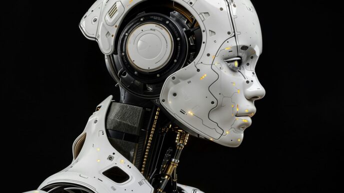

You know how AI is getting bigger and faster all the time? Well, the way computers move data around is starting to struggle to keep up. Think of it like trying to pour a whole lake through a tiny straw. That’s where Ayar Labs comes in. They’re working on a new way to send data using light, which is way faster and uses less power than the old electrical wires. This could be a really big deal for making AI work even better.
Key Takeaways
- Ayar Labs is developing optical interconnects, a new technology that uses light to move data, to solve the growing problem of data bottlenecks in AI systems.
- Their technology, like the SuperNova™ remote light source and TeraPHY™ optical I/O chiplet, aims to make AI infrastructure more efficient and less power-hungry.
- By using open standards like UCIe, Ayar Labs is working to make their optical solutions compatible with existing and future AI hardware.
- The company has built strong partnerships with major tech players and manufacturers, which is helping to move their optical technology from research to real-world use.
- Ayar Labs’ innovations are expected to significantly change how AI systems are built, leading to faster performance and lower costs in data centers.
Ayar Labs: Pioneering Optical Interconnects for AI
The Genesis of Ayar Labs
Back in 2015, Ayar Labs started with a pretty big idea. The folks who founded it were researchers, and they saw something coming. They noticed that while computer chips were getting faster and denser, the way they talked to each other – the connections, or interconnects – wasn’t keeping up. It was like having a super-fast brain but only being able to whisper messages. This gap was especially clear when looking at the future, particularly with the rise of AI. The team realized that the old way of doing things, using copper wires, just wouldn’t cut it for the massive amounts of data AI needs to process. They thought, "What if we could use light instead of electricity?" It was a bold thought, especially back then, but they were convinced it was the only way forward.
Addressing the Connectivity Bottleneck
So, what’s this "connectivity bottleneck"? Imagine a huge AI model, like the ones that can generate text or images. These models need to move enormous amounts of data between different parts of the system – the processors, the memory, and so on. Traditional electrical connections, the ones using copper, have limits. They can only carry so much data, and the further the data has to travel, the slower and less efficient it becomes. This is the bottleneck. It means that even if you have incredibly powerful processors, they can get held up waiting for data. Ayar Labs saw this problem coming years ago, back when they were still in university research. They looked at how data moved and realized that the limitations of electrical signals were going to become a major roadblock for future computing, especially for AI and high-performance computing.
Inventing Optical Connectivity for Compute Fabrics
This is where Ayar Labs really started to innovate. Instead of just thinking about networking over long distances, they focused on making optical connections work right inside the computer, between chips. They developed new ways to put tiny optical components onto silicon chips, alongside the regular electronic parts. Think of it like integrating a tiny laser and light detector directly onto the same piece of silicon as your processor. Their big breakthrough was creating the first microprocessor that could actually talk to memory using light. This was a huge step because it showed that optical communication wasn’t just for long-distance phone calls; it could be used for the super-fast, short-distance communication needed within a computer. Founding Ayar Labs in 2015 was all about taking that academic breakthrough and making it a reality for data centers and AI systems.
The Evolution of Ayar Labs’ Technology
When Ayar Labs first started back in 2015, the world of data centers wasn’t quite ready for what they had in mind. The initial ideas were actually geared more towards military applications, think drones and satellites where you need top performance in a small, light package. But then, AI really started to take off, and suddenly, the focus shifted dramatically towards data centers. It became clear that the way we move data around inside these massive computing hubs was becoming a major roadblock for anything AI-related.
Early Challenges and Strategic Opportunities
In those early years, from about 2015 to 2018, the industry just wasn’t set up for Ayar’s optical interconnects. There were missing pieces in manufacturing, assembly, and testing. Plus, there wasn’t a big, high-volume market application that would get everyone excited and working together. But Ayar’s team was smart. They saw a few key trends that would shape their future:
- Chipletization: As making single, giant chips got harder and more expensive, companies like AMD and Intel started breaking their processors down into smaller, interconnected pieces called chiplets. This opened the door for Ayar to create their own optical chiplets.
- Manufacturing Advances: Big chip makers like GlobalFoundries, Intel Foundry, and TSMC were getting better at working with silicon photonics, which is basically using light to send signals on chips. This was exactly what Ayar needed.
- The Rise of AI Workloads: The explosion in AI, with specialized chips like Google’s TPUs and custom silicon from startups, pointed towards a future where systems would be more spread out and need way more connections.
Chipletization and Manufacturing Advances
These trends were a big deal. The move towards chiplets meant that integrating new kinds of components, like optical ones, became more feasible. Instead of trying to build a whole new system from scratch, Ayar could focus on creating optical components that fit into these emerging chiplet designs. This made the technology much more adaptable. At the same time, the foundries were improving their silicon photonics processes. This meant they could produce the complex optical components Ayar needed with better reliability and at a larger scale. It was a perfect storm of technological progress.
The Rise of AI Workloads
But the real game-changer was AI. As AI models got bigger and more complex, the amount of data they needed to process exploded. Traditional electrical connections just couldn’t keep up. They were too slow, used too much power, and created too much heat. Ayar Labs recognized that optical interconnects, which use light to transmit data, were the only way to break through this bottleneck. This realization, happening around 2018, led Ayar to make a big bet: that large-scale AI systems would become the dominant force in data centers, and optical I/O would be absolutely critical for making them work efficiently and affordably.
Revolutionizing AI Infrastructure with Optical I/O
The way we build and run AI systems is changing, and fast. You know, with all these massive AI models getting bigger and more complex, the old ways of moving data just aren’t cutting it anymore. We’re hitting a wall, and that’s where Ayar Labs’ optical I/O technology comes in. It’s a pretty big deal because it lets data move way faster and with less power than the old copper wires.
Ayar Labs’ In-Package Optical I/O Solution
So, what exactly is Ayar Labs doing? They’ve figured out how to put optical connections right into the same package as the computer chips themselves. Think of it like this: instead of data having to travel a long distance over copper, it can now take a super-short optical path. This makes a huge difference. It means we can pack more computing power together without getting bogged down by slow data transfers. This approach is key to making AI training and running these models much more efficient. It’s not just about speed, though; it’s also about cutting down on the energy needed to move all that data around.
Maximizing Compute Efficiency and Performance
When you can move data faster and with less delay, your processors aren’t sitting around waiting. This means they can do more work, more quickly. For AI, this translates directly into faster training times for models and quicker responses when the AI is actually being used. We’re talking about systems that can handle much larger problems than before. It’s like upgrading from a dirt road to a superhighway for your data. This jump in performance is what allows us to build and deploy the next generation of AI applications.
Reducing Costs and Power Consumption
Moving data with light is just more efficient than doing it with electricity over copper, especially over longer distances within a system. Less energy used means lower electricity bills for data centers, which is a big deal when you’re running thousands of these machines. Plus, by making systems more compact and efficient, we can potentially reduce the physical space and cooling needed. This all adds up to a more economical way to build and operate AI infrastructure. It’s a win-win for performance and the bottom line. The development of technologies like Optical Circuit Switches also plays a role in this efficiency push.
Key Innovations from Ayar Labs
Ayar Labs didn’t just come up with a new idea; they built the actual hardware to make optical connections a reality for AI. They’ve got a couple of big things that really stand out.
The SuperNova™ Remote Light Source
Think of this as the engine that powers the whole optical system. It’s a separate unit that generates the light signals needed for data transfer. What’s neat about it being ‘remote’ is that it can be placed away from the main compute chips. This helps keep the chips themselves cooler and more efficient, which is a big deal when you’re running massive AI models. It’s designed to be compact and use less power than older methods, which adds up quickly in a data center.
TeraPHY™ Optical I/O Chiplet
This is the heart of the operation, a tiny chiplet that handles the optical input and output. It’s designed to work directly with the main processors, like CPUs and GPUs, often sitting right alongside them. The TeraPHY chiplet is the industry’s first optical I/O solution that’s built to be integrated directly into the package with the compute silicon. This close integration is what allows for incredibly fast data movement between chips, far beyond what traditional electrical connections can manage. It’s built using silicon photonics, a technology that uses light to send data over tiny optical pathways etched into silicon.
Integration with Universal Chiplet Interconnect Express (UCIe)
This is where Ayar Labs is playing nice with others. UCIe is an open industry standard for how different chiplets can talk to each other. By making their TeraPHY chiplet compatible with UCIe, Ayar Labs is making it easier for their optical technology to be adopted. It means that companies building AI systems don’t have to create entirely new, proprietary ways to connect their chips; they can use a standard that many are already adopting. This makes the whole process simpler and more scalable for everyone involved.
Here’s a quick look at what these innovations bring:
- Speed: Optical connections are significantly faster than electrical ones.
- Efficiency: Less power is needed to move data over optical links.
- Scalability: Enables larger and more complex AI systems to be built.
- Compatibility: Adherence to standards like UCIe makes integration smoother.
Strategic Partnerships Driving Ayar Labs’ Growth
Collaborations with Compute Leaders
It’s pretty clear that Ayar Labs isn’t doing this alone. They’ve been busy building relationships with some of the biggest names in computing. Think about it, getting technology like this into the hands of people who actually build AI systems means you need buy-in from the folks making the processors and the servers. Companies like AMD and NVIDIA, who are pretty much the kings of AI chips right now, are involved. This isn’t just about them saying "nice job"; it’s about making sure Ayar’s optical I/O fits into their future plans. It’s like getting the stamp of approval from the main players, which is a huge deal for any new tech.
Manufacturing and Assembly Ecosystem
Beyond just the chip designers, Ayar Labs is also working with the companies that actually make the chips and put everything together. We’re talking about foundries like GlobalFoundries and Intel Foundry, and even places like TSMC. These partnerships are super important because Ayar’s technology needs to be manufactured at a large scale. It’s not enough to have a cool idea; you need to be able to produce it reliably and in big numbers. They’re also building out their assembly partners, which means they’re setting up the whole supply chain to get their optical interconnects ready for the real world.
Supporting Industry Standards
One of the smartest things Ayar Labs seems to be doing is playing nice with industry standards, like the Universal Chiplet Interconnect Express (UCIe). This is a big deal because it means their technology isn’t some proprietary black box. When you build things using open standards, it makes it way easier for other companies to adopt your tech. It lowers the barrier to entry and makes everyone more comfortable. This commitment to open standards is probably a major reason why so many big companies are willing to partner with them. It means Ayar’s optical solutions can be integrated more easily into existing and future systems without causing a massive headache for everyone involved.
The Future of Data Centers with Ayar Labs
Transforming System-Level AI Architectures
So, what does all this mean for the future? It’s pretty clear that the way we build and think about data centers is going to change, especially for AI. Right now, a lot of the performance we get is limited by how fast data can move around. Ayar Labs’ optical I/O is like building superhighways for data instead of tiny country roads. This means we can connect more processors, more memory, and do it all much faster. Think about it: instead of having a bunch of separate parts that are slow to talk to each other, we can create more integrated systems where everything works together smoothly. This isn’t just about making things a little faster; it’s about enabling entirely new ways to design AI systems that can handle much bigger and more complex problems than we can today.
Phased Adoption of Optical Solutions
It’s not like every data center will switch to optical overnight. That wouldn’t make much sense. Instead, we’re going to see a gradual shift. Initially, you’ll find these optical connections in the most demanding AI applications – the ones that really push the limits of current technology. These are the places where the speed and efficiency gains are most needed and where the investment makes the most sense. As the technology matures and becomes more widespread, and as more companies get comfortable with it, it will start appearing in more general-purpose AI tasks. It’s a bit like how solid-state drives (SSDs) first showed up in high-performance computers before becoming standard in almost every laptop and desktop.
Here’s a rough idea of how this might play out:
- Early Adopters: High-performance computing (HPC) and large-scale AI training clusters will be the first to widely adopt optical interconnects. These environments have the most to gain from reduced latency and increased bandwidth.
- Expansion: As costs come down and the ecosystem grows, optical solutions will become more common in AI inference servers and other specialized compute environments.
- Mainstream Integration: Eventually, optical I/O could become a standard component in many types of servers, much like current electrical interconnects, enabling more efficient and powerful general computing.
Enabling Next-Generation AI Infrastructure
Ultimately, Ayar Labs is paving the way for the next wave of AI. The current limitations in data movement are a major roadblock for developing more advanced AI models and applications. By solving this bottleneck with optical technology, Ayar Labs is helping to remove those barriers. This means researchers and developers can focus on building smarter AI, not just figuring out how to make the hardware keep up. The ability to move data at the speed of light is what will allow AI to continue its rapid progress. We’re talking about AI that can understand and process information in ways we can only imagine right now, powering everything from scientific discovery to more personalized digital experiences. It’s a pretty exciting time to be thinking about the future of computing.
Looking Ahead
So, it’s pretty clear that Ayar Labs isn’t just tinkering around the edges. They’ve really gone and built something that could change how data centers work, especially with all this AI stuff exploding. By using light instead of wires to move data around, they’re tackling a big problem that’s been holding things back. It’s not just about making things faster, but also about using less power and making everything more efficient. We’re seeing a lot of big players getting on board, which tells you something. It feels like we’re at the start of a big shift, and Ayar Labs seems to be leading the charge. It’ll be interesting to see how this all plays out in the next few years as more systems start using this optical tech.
Frequently Asked Questions
What is Ayar Labs and what do they do?
Ayar Labs is a company that makes special connections for computers. Think of it like super-fast highways for data inside computers and data centers. They use light, like in fiber optic cables, to move information much quicker than old-fashioned wires can.
Why is Ayar Labs’ technology important for AI?
Artificial intelligence (AI) needs to move huge amounts of data very quickly. As AI programs get bigger and more complex, regular computer connections get overloaded, like a traffic jam. Ayar Labs’ light-based connections are like adding many more lanes to the highway, allowing AI to work much faster and more efficiently.
What is optical I/O?
Optical I/O means using light to send data in and out of computer chips. Instead of electricity traveling through copper wires, tiny beams of light carry the information. This is way faster, uses less energy, and can send more data at once.
What are chiplets, and how do they relate to Ayar Labs?
Chiplets are like small, specialized building blocks for computer chips. Ayar Labs creates optical connections that can link these chiplets together using light. This allows designers to build more powerful and efficient chips by connecting these smaller pieces seamlessly.
What are SuperNova and TeraPHY?
SuperNova is a special light source made by Ayar Labs that powers their optical connections. TeraPHY is a chiplet that uses this light to send and receive data super fast. Together, they are key parts of Ayar Labs’ technology for speeding up AI.
How does Ayar Labs help save energy and money?
By using light instead of electricity for data transfer, Ayar Labs’ technology uses much less power. This means data centers can save a lot on electricity bills. Also, by making AI work more efficiently, it can reduce the need for as many expensive computer parts, saving money in the long run.