I was reading about tsmc’s newest 3nm process and thought I’d share why it matters. They hit some crazy tech milestones, and those tiny chips are powering next-gen AI and data centers. Plus, tsmc’s beefing up fabs around the world and teaming up with designers to make it all work. Oh, and they’re also trying to be greener. Here’s what jumped out at me.
Key Takeaways
- tsmc pulled off sub-3nm scaling by adding new EUV tools and tweaking their process to boost yields
- Those 3nm chips run faster and use less power, which is a big win for AI and high-performance computing
- tsmc is opening more fabs in Taiwan, the US, Japan, and Europe to meet demand and handle supply hiccups
- Teaming up with EDA vendors and IP providers helped turn complex 3nm SoC designs into real products
- The new fabs focus on cutting waste, saving water, and adding solar and wind to shrink the environmental footprint
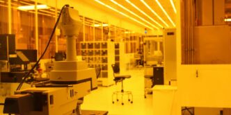
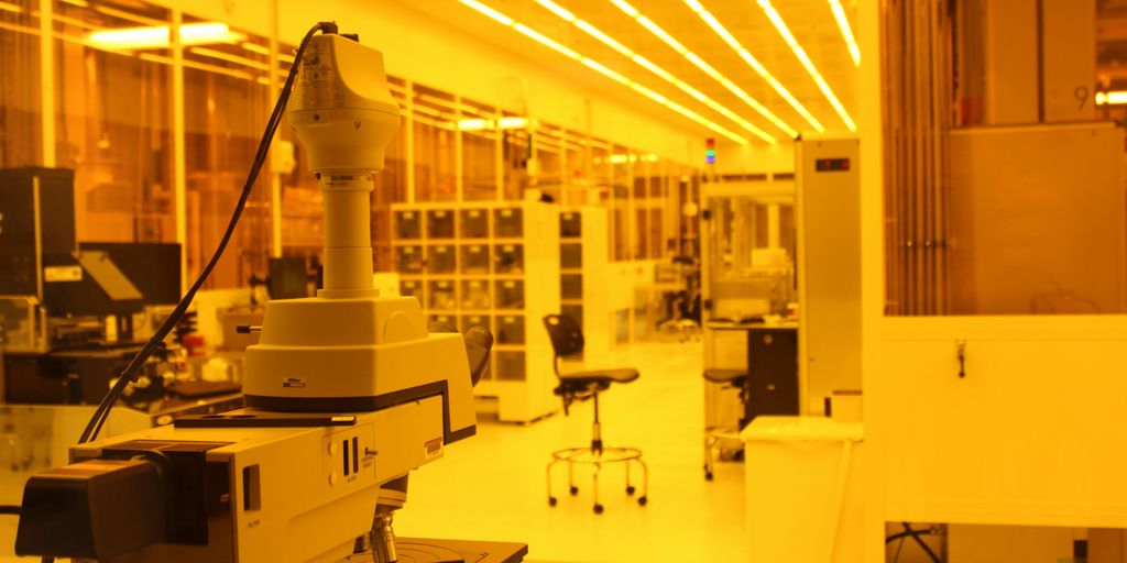
TSMC’s 3nm Breakthrough And Its Technical Milestones
TSMC’s 3nm node is a big deal, not just a minor upgrade. It represents a significant leap forward in semiconductor technology. It’s not easy shrinking things down to this size, and TSMC had to overcome some serious hurdles to get here. They’re not just making chips smaller; they’re making them more powerful and efficient. This node is expected to power a whole new generation of devices, from smartphones to data centers. It’s a testament to TSMC’s engineering prowess and their commitment to pushing the boundaries of what’s possible. TSMC’s success is also a win for companies like Apple, who rely on their advanced manufacturing capabilities. TSMC’s 3nm process is a game-changer.
Challenges In Achieving Sub-3nm Scaling
Getting to 3nm wasn’t a walk in the park. The physics get really tricky at that scale. Think about it: we’re talking about features that are only a few atoms wide! One of the biggest problems is dealing with quantum effects, where electrons start behaving in unpredictable ways. Then there’s the issue of variability – making sure every chip performs consistently when they’re all so tiny. And of course, there’s the cost. Developing these advanced processes requires huge investments in R&D and equipment. It’s a constant balancing act between performance, cost, and manufacturability. TSMC has been investing heavily to stay ahead. They’ve had to develop new materials, new manufacturing techniques, and new ways of testing and validating their designs. It’s a truly impressive feat of engineering.
Innovations In EUV Lithography Deployment
EUV lithography is key to making 3nm chips a reality. EUV, or extreme ultraviolet, uses light with a really short wavelength to print the tiny patterns on silicon wafers. But EUV machines are incredibly complex and expensive. They’re also not perfect. TSMC has had to innovate to get the most out of EUV. They’ve developed new ways to optimize the EUV process, reduce defects, and improve throughput. They’ve also worked closely with ASML, the company that makes EUV machines, to push the technology forward. TSMC’s expertise in EUV deployment is a major competitive advantage. It’s one of the reasons why they’re ahead of other foundries in the race to advanced nodes.
Yield Enhancement Through Process Calibration
Even with the best technology, making chips is still a game of probabilities. Not every chip that comes off the line is going to work perfectly. That’s why yield is so important. Yield refers to the percentage of chips that meet specifications. TSMC has developed sophisticated techniques for process calibration to maximize yield. This involves carefully monitoring every step of the manufacturing process and making adjustments to optimize performance. They use advanced data analytics and machine learning to identify and correct problems. Improving yield is crucial for controlling costs and ensuring that they can meet customer demand. TSMC’s fab investments are paying off.
Harmonizing Design And Manufacturing Rules
Designing chips for advanced nodes like 3nm is a collaborative effort. Chip designers and manufacturers need to work closely together to ensure that designs can be reliably manufactured. This means establishing clear design rules that take into account the limitations of the manufacturing process. TSMC works closely with its customers to develop these rules and provide them with the tools and support they need to design successful chips. This co-optimization of design and manufacturing is essential for achieving high performance and yield. It’s a key part of TSMC’s open innovation platform and their commitment to customer success. The company’s history shows a commitment to innovation.
Transforming AI And High-Performance Computing With TSMC’s 3nm Chips
TSMC’s 3nm process is a game-changer, especially for AI and high-performance computing (HPC). It’s not just about shrinking transistors; it’s about unlocking new levels of power and efficiency that are critical for the next generation of tech. Think faster AI, more powerful data centers, and smarter edge devices. It’s a big deal.
Power Efficiency Gains For Next-Gen AI Workloads
AI is power-hungry. Training those massive models and running complex algorithms takes a ton of energy. TSMC’s 3nm chips are designed to sip power, not gulp it. This means longer battery life for devices and lower energy bills for data centers. The improvements are significant. For example, early tests show a 25-30% reduction in power consumption for certain AI tasks compared to the previous generation. That’s huge when you’re talking about the scale of modern AI.
Performance Boosts In Data Center Accelerators
Data centers are the backbone of the digital world, and they’re constantly pushing the limits of performance. TSMC’s 3nm process allows for denser and faster chips, which translates directly into faster processing speeds for data center accelerators. This is crucial for handling the ever-increasing demands of AI, cloud computing, and big data analytics. The demand for high-performance computing is only going to increase. We’re talking about a serious upgrade in capabilities.
Tailoring SoC Designs For Emerging Machine Learning Models
One size doesn’t fit all, especially when it comes to machine learning. TSMC’s 3nm process gives chip designers more flexibility to tailor their system-on-a-chip (SoC) designs to specific machine learning models. This means they can optimize for performance, power efficiency, and cost, depending on the application. It’s about creating the perfect chip for the job, whether it’s image recognition, natural language processing, or something else entirely. This level of customization is a big advantage.
Edge AI Use Cases Enabled By Miniaturization
Edge AI is all about bringing AI processing closer to the source of the data, whether it’s a smartphone, a drone, or a smart sensor. TSMC’s 3nm process makes it possible to pack more processing power into smaller devices, which is essential for edge AI applications. This opens up a whole new world of possibilities, from real-time image analysis to autonomous vehicles. The benefits are clear:
- Faster response times
- Reduced latency
- Improved privacy
It’s a game-changer for the Internet of Things and beyond.
Scaling Global Production Through TSMC’s Strategic Fab Investments
TSMC isn’t just sitting still; they’re making some serious moves to ramp up production globally. It’s all about meeting the growing demand for advanced chips, especially those using their cutting-edge 3nm process. They’re spreading their manufacturing footprint to stay ahead of the curve.
Expanding Capacity In Taiwan’s Leading Facilities
TSMC is still heavily invested in its home base. A large chunk of their capital expenditure is going towards expanding existing fabs and building new ones in Taiwan. This includes facilities dedicated to the 3nm process and even looking ahead to 2nm and A16 nodes. They’re not just building more of the same; they’re upgrading to handle the most advanced chip tech. In 2025, TSMC plans to open nine new sites, including eight wafer fabs. This expansion ensures they can keep up with the demand from major players like Nvidia, Apple, and AMD.
Collaborative Ventures In Overseas Manufacturing
TSMC is making a big push overseas, especially in the United States, Japan and Germany. These collaborative ventures are key to diversifying their manufacturing base and semiconductor supply chains. By 2030, TSMC’s total investment in the US will reach an estimated $165 billion, supporting the construction of five major fabs, two advanced packaging plants, and a major R&D center in Arizona. These plants aren’t just about making chips; they’re about building a more resilient and geographically diverse supply chain. It’s a strategic move to address global demand and geopolitical considerations.
Subsidy-Driven Growth In Key Markets
Government incentives are playing a big role in TSMC’s expansion plans. Countries are offering subsidies and other support to attract semiconductor manufacturing. This helps offset the high costs of building and operating advanced fabs. It’s a win-win: TSMC gets financial support, and the host countries get a boost to their tech sectors. This subsidy-driven growth is particularly evident in the US, where the government is keen to bring chip manufacturing back home. These subsidies are helping TSMC accelerate its expansion and advanced packaging capabilities.
Ensuring Supply Chain Resiliency
One of the biggest drivers behind TSMC’s global expansion is the need for a more resilient supply chain. Recent events have highlighted the risks of relying too heavily on a single region for chip production. By diversifying their manufacturing locations, TSMC is reducing its vulnerability to disruptions caused by natural disasters, geopolitical tensions, or other unforeseen events. This ensures that their customers can continue to get the chips they need, no matter what happens. TSMC’s expansion in Arizona is not merely about increasing production capacity—it is a strategic response to global supply chain restructuring, explosive demand for AI-era chips, and the growing pressure from U.S.-China tech tensions to "de-risk" from China and Taiwan.
Ecosystem Collaborations Fueling TSMC’s 3nm Design Excellence
TSMC’s 3nm process isn’t just about what happens inside their own fabs. A huge part of their success comes from how well they work with other companies in the industry. It’s a whole ecosystem thing, and it’s what allows them to push the boundaries of what’s possible. These partnerships are essential for optimizing chip designs and ensuring everything runs smoothly from start to finish.
Partnership Models With EDA And IP Vendors
TSMC doesn’t do it alone. They team up with Electronic Design Automation (EDA) and Intellectual Property (IP) vendors. Think of it like this: EDA vendors provide the software tools that chip designers use, and IP vendors provide pre-designed components that can be plugged into a chip design. TSMC works closely with these vendors to make sure their tools and IP are optimized for the 3nm process. This means faster design cycles, fewer errors, and better overall chip performance. It’s a win-win for everyone involved. These technology hotspots are crucial for innovation.
Co-Optimization With Chip Architects
It’s not just about the tools; it’s about the people using them. TSMC works hand-in-hand with chip architects from companies like Apple, Nvidia, and Qualcomm. This co-optimization is key. TSMC provides feedback on the manufacturability of designs, and the chip architects provide feedback on the performance characteristics of the process. This back-and-forth helps to refine the design and the process, resulting in chips that are both high-performing and manufacturable. It’s a collaborative effort that leverages the strengths of both parties.
Integrated IP Libraries For Complex SoCs
System-on-a-Chip (SoC) designs are getting more and more complex. To make things easier, TSMC offers integrated IP libraries. These libraries contain a wide range of pre-designed components that can be easily integrated into an SoC design. This saves designers time and effort, and it also helps to ensure that the chip will work as expected. TSMC’s IP libraries are constantly being updated to reflect the latest advances in technology. Here are some benefits of using integrated IP libraries:
- Reduced design time
- Lower risk of errors
- Improved chip performance
- Faster time to market
Testing And Validation Synergies
Before a chip goes into production, it needs to be thoroughly tested and validated. TSMC works with its partners to develop comprehensive testing and validation methodologies. This includes everything from basic functionality testing to advanced stress testing. The goal is to identify any potential problems before the chip is released to customers. This helps to ensure that the chips are reliable and meet the required performance specifications. It’s a critical step in the chip development process.
Economic Impact And Market Dynamics Of TSMC’s Advanced Nodes
Pricing Strategies For High-End Consumer Devices
Okay, so let’s talk money. TSMC’s 3nm chips aren’t exactly cheap, and that cost trickles down to the consumer. Think about the latest smartphones, high-end laptops, and gaming consoles. The advanced node technology significantly impacts their price tags. It’s a balancing act for manufacturers: how much performance can they squeeze in while keeping the price somewhat reasonable? We’re seeing companies explore different tiers of products, with the very top end sporting the newest chips and a corresponding premium price. It’s a game of perceived value, and consumers are definitely feeling the pinch.
Competitive Landscape Among Global Foundries
TSMC isn’t the only player in the foundry game, but they’re definitely leading the pack. Samsung is their main competitor, and they’re constantly trying to catch up. Then you’ve got Intel, who’s been trying to get back into the game for a while now. The competition is fierce, and it’s driving innovation, but it also creates a lot of pressure. Everyone’s racing to get to the next node first, and that can lead to some interesting decisions. The SD-WAN market is also growing, which adds another layer of complexity to the competitive landscape. It’s a high-stakes game, and the winners will be the ones who can deliver the best performance at the best price.
Long-Term Return On Investment For Major Clients
For companies like Apple, Nvidia, and AMD, investing in TSMC’s advanced nodes is a huge gamble. They’re betting that the performance gains will justify the increased cost. It’s not just about bragging rights; it’s about delivering a better product that customers are willing to pay for. The return on investment isn’t always immediate, but over the long term, it can be significant. Think about the iPhone – Apple’s ability to leverage TSMC’s technology has been a major factor in their success. It’s a long-term game, and the companies that can see the big picture are the ones that will come out on top.
Demand Forecast For Next-Generation Electronics
Everyone wants the latest and greatest tech, right? That demand is what fuels TSMC’s growth. As AI, VR, and other emerging technologies become more prevalent, the demand for advanced chips will only increase. TSMC is betting big on this trend, and they’re investing heavily in new fabs to meet the expected demand. But forecasting demand is tricky. There are so many factors that can influence it, from economic conditions to geopolitical events. It’s a constant balancing act, and TSMC needs to be able to adapt quickly to changing market conditions.
Here’s a quick look at projected growth in key sectors:
- AI Processors: Expected to grow by 30% annually over the next 5 years.
- High-Performance Computing: Driven by data center expansion, with a 25% annual growth rate.
- Automotive Electronics: Electric vehicles and autonomous driving are fueling a 20% annual increase in demand.
Sustainability And Energy Efficiency In TSMC’s Cutting-Edge Fabs
It’s no secret that making chips takes a lot of energy and resources. TSMC, being the giant it is, has a big responsibility to minimize its impact. They’re not just doing it because it’s the right thing to do; it also makes good business sense. Cutting waste and using resources more efficiently saves money and attracts customers who care about sustainability. It’s a win-win, really.
Water Recycling And Conservation Initiatives
Water is super important in chip manufacturing. It’s used for cleaning wafers and cooling equipment. TSMC is working hard to reduce its water usage through recycling and conservation. They’re implementing advanced water treatment technologies to reuse water multiple times within their fabs. This not only reduces their reliance on freshwater sources but also minimizes wastewater discharge. It’s a big deal, especially in regions where water is scarce. TSMC’s water conservation efforts are pretty impressive.
Renewable Energy Integration In Fabrication Plants
TSMC is making a push to power its fabs with renewable energy sources. This includes solar, wind, and other clean energy options. By integrating these sources into their energy mix, they’re reducing their carbon footprint and dependence on fossil fuels. It’s a long-term investment that will pay off in terms of both environmental impact and cost savings. They’re also exploring partnerships with renewable energy providers to secure a stable supply of clean power. It’s a complex undertaking, but they seem committed to making it work.
Waste Reduction In Chemical And Material Usage
Chip manufacturing involves a lot of chemicals and materials, and waste is inevitable. TSMC is focused on reducing this waste through process optimization and material substitution. They’re finding ways to use fewer chemicals, recycle materials, and dispose of waste responsibly. This not only reduces their environmental impact but also lowers their operating costs. It’s a continuous improvement process that requires constant innovation and attention to detail. They’re also working with suppliers to ensure that materials are sourced sustainably. Here’s a quick look at their waste reduction targets:
- Reduce chemical usage by 15% by 2030
- Increase material recycling rate to 80% by 2030
- Eliminate hazardous waste discharge by 2035
Carbon Footprint Mitigation Strategies
TSMC is actively working to reduce its carbon footprint through a variety of strategies. This includes improving energy efficiency, using renewable energy, and reducing waste. They’re also investing in carbon offset projects to compensate for emissions they can’t eliminate. It’s a comprehensive approach that addresses all aspects of their operations. They’re setting ambitious targets and tracking their progress closely. It’s a challenging task, but they seem determined to meet their goals. TSMC’s carbon mitigation strategies are pretty comprehensive.
## Conclusion
Wrapping up, TSMC’s move to 3nm isn’t just about squeezing more transistors into a tiny space. It’s the secret sauce behind faster phones, smarter AI, and more power in sleek gadgets. Sure, the costs and technical headaches are real. But by opening new fabs in Taiwan, Arizona, Japan, and Germany, they’re showing it can pay off. For anyone tracking the next wave of tech, keep an eye on those 3nm lines. They may look like a small step in a chip plant, but they’re driving the big changes we’ll see in the years ahead.
Frequently Asked Questions
What is TSMC’s 3nm process?
The 3nm process is TSMC’s newest way to make computer chips with super tiny parts. Smaller parts help chips run faster and use less power.
Why does the 3nm process matter for AI and big computers?
3nm chips can handle lots of calculations very quickly. That speed boost makes AI programs smarter and data centers more powerful.
How did TSMC overcome the challenges of making 3nm chips?
They used a special light tool called EUV, tweaked their factory steps to reduce defects, and matched chip designs closely with their manufacturing rules.
Where will TSMC build its 3nm chips?
Most 3nm chips come from TSMC’s fabs in Taiwan. The company is also building new factories in the U.S., Japan, and Germany to spread production.
Will 3nm chips cost more than older chips?
At first, they are pricier because of fancy equipment and research costs. But as TSMC adds more factories and makes more chips, prices should drop over time.
How is TSMC making 3nm production more eco-friendly?
They recycle and clean water, add more renewable energy like solar, and cut down on chemical waste to lower their carbon footprint.