So, you’re trying to get a handle on chip BGA technology? It’s pretty much everywhere in our gadgets these days, from phones to more serious equipment. Basically, it’s a way to pack a lot of connections into a small space using little solder balls. We’ll break down what makes BGA tick, why it’s so common, and what goes into making it work right. It’s not always straightforward, but understanding the basics really helps.
Key Takeaways
- Chip BGA packaging uses solder balls underneath the chip to connect to a circuit board, allowing for more connections in a smaller space.
- The BGA substrate is the base for these connections, and the materials used affect performance and heat handling.
- Advanced techniques like micro-BGA and underfill help improve density and reliability, especially for demanding applications.
- Getting BGA soldering right involves careful attention to reflow profiles, solder paste choice, and designing the board layout for easier assembly.
- Challenges like rework difficulty and inspection issues are common with chip BGA, but modern tools and techniques offer solutions.
Understanding Ball Grid Array Technology
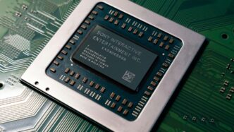
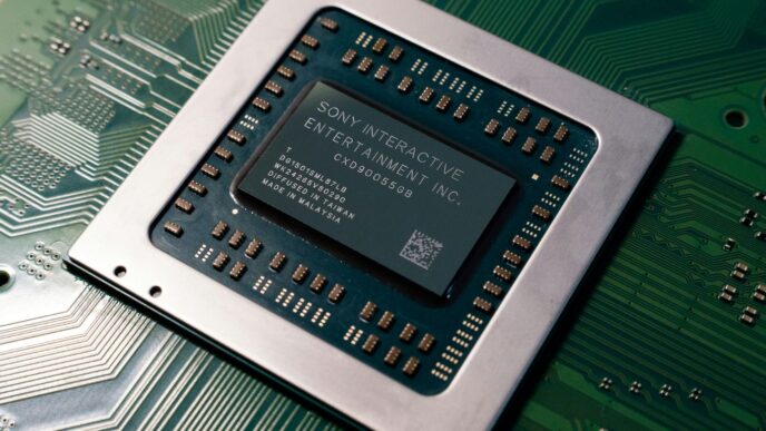
So, what exactly is this Ball Grid Array, or BGA, thing we keep hearing about in electronics? Basically, it’s a way to package computer chips. Instead of having little legs sticking out all around the edges like older chips, BGAs have a whole bunch of tiny solder balls on the bottom, arranged in a grid. This setup lets you cram way more connections onto a chip, which is pretty neat when you’re trying to make things smaller and faster. It’s a big deal in modern electronics because it helps with how well the chip handles heat too.
What is Chip BGA?
A Ball Grid Array (BGA) is a type of surface-mount packaging for integrated circuits (ICs). Think of it as a neat little box for a chip that connects to a circuit board using a grid of solder balls on its underside. This is different from older styles of chips that had pins sticking out around the edges. The BGA design allows for a lot more connections in a smaller space, which is why it’s used in so many complex and high-performance electronic devices today. It’s a key part of how we get powerful gadgets that are also quite compact. You can find out more about what a BGA is if you’re curious.
The Role of BGA in Modern Electronics
BGAs have become really important in the electronics world. They let us pack more functionality into smaller devices, which is why your smartphone or laptop can do so much. The way BGAs are designed, with all those solder balls underneath, means they can handle more signals and power compared to older chip packages. This is especially important for things like high-speed processors and memory chips where lots of data needs to move quickly and reliably. They also help manage heat better, which is a constant challenge when you’re trying to make electronics more powerful and smaller at the same time.
Key Advantages of BGA Packaging
Why do manufacturers like using BGAs so much? Well, there are a few big reasons:
- Higher Connection Density: With balls arranged in a grid on the entire underside, you can fit many more connections than with edge-based pins. This is great for chips that need to do a lot.
- Improved Thermal Performance: The larger area for connections also helps spread out the heat generated by the chip, making it easier to keep things cool.
- Smaller Footprint: Because the connections are underneath, the overall package can be smaller and flatter, which is a win for making devices more compact.
- Better Electrical Performance: Shorter connections from the balls to the chip can lead to better signal integrity, especially at high speeds.
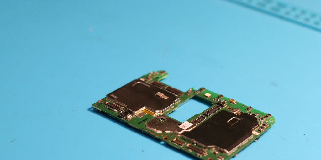
Core Components and Materials of BGA
When we talk about Ball Grid Array (BGA) technology, it’s easy to get caught up in the solder balls themselves, but there’s a lot more going on under the hood. The real workhorse, the foundation that makes all those connections possible, is the BGA substrate. Think of it as the intricate road map for all the electrical signals and power flowing through the chip.
The BGA Substrate: Foundation of Connectivity
The substrate is basically a specialized board, usually made of laminate or ceramic material. It’s where you find all those little pads arranged in a grid. These pads are the connection points for the solder balls that will eventually attach the whole BGA package to the main printed circuit board (PCB). It’s the intermediary, connecting the actual silicon chip to the outside world. Getting the substrate design right is super important for how well the whole electronic device performs and how long it lasts. It’s not just about making connections; it’s also about managing heat and keeping signals clean.
Materials Used in BGA Substrates
So, what are these substrates actually made of? It really depends on what the chip needs to do.
- FR-4 Laminate: This is a pretty common choice because it’s not too expensive and works well with standard PCB manufacturing. It’s made from woven glass fabric and epoxy resin, offering decent electrical insulation and strength.
- High-Temperature Laminates: If the device is going to get hot, these are a better bet. They can handle higher operating temperatures without breaking down.
- Ceramic: For really demanding applications, like high-frequency or high-power stuff, ceramic substrates are great. They’re really good at insulating electrically and also do a good job of moving heat away from the chip.
- Organic Substrates: These offer a middle ground, balancing electrical performance, cost, and how easy they are to work with.
The choice of material directly impacts how well the device handles heat and how clean the electrical signals stay. It’s a big decision that affects the overall reliability of the electronics. You can find more details on BGA packaging technology.
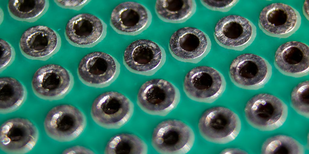
Solder Balls: The Interconnect Medium
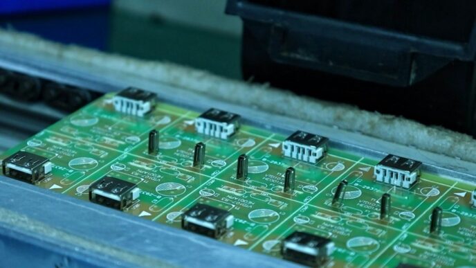
These little spheres of solder are what make the BGA package physically connect to the PCB. They’re arranged in that characteristic grid pattern on the underside of the substrate. Each solder ball is precisely placed to align with a corresponding pad on the PCB. During the soldering process, these balls melt and form strong electrical and mechanical connections. The size and spacing of these balls are critical for high-density interconnects, allowing more connections in a smaller space compared to older packaging methods. Getting the solder joint right is key; too little solder means a weak connection, and too much can cause shorts. The quality of these connections is what allows signals and power to flow reliably between the chip and the rest of the system. It’s a pretty neat system when it all works correctly.
Advanced BGA Packaging Techniques
As electronics get smaller and faster, the way we package chips has to keep up. This is where advanced BGA techniques come into play, pushing the boundaries of what’s possible. We’re talking about making things denser, improving how signals travel, and making sure everything stays cool and reliable, even under tough conditions.
Micro-BGA and Ultra-Fine Pitch BGA
Think about the space inside your smartphone or a tiny medical device. To fit everything in, we need smaller components with more connections packed closer together. That’s what Micro-BGA and Ultra-Fine Pitch BGA are all about. They use smaller solder balls and have a much tighter spacing between them, which means more connections in a smaller area. This is a big deal for increasing component density, letting us pack more features into less space. Plus, these shorter connections can actually improve how fast signals move, which is great for high-speed stuff. It also helps with heat management, as the smaller balls can help spread heat out better. This is a key area for anyone looking to shrink their designs while keeping performance high. It’s all about getting more bang for your buck in terms of space and speed.
Flip Chip Technology Integration
Another big step forward is flip chip technology. Instead of the usual way of connecting a chip, here the chip is flipped upside down. The solder balls on the chip connect directly to the circuit board. This might sound simple, but it makes a big difference. Because the connections are so much shorter, signals don’t get lost or slowed down as much. This is super important for chips that do a lot of heavy lifting, like processors or high-frequency communication chips. It also helps with cooling because the chip can transfer heat more directly to the board. This method allows for really compact designs, which is a win for any product where space is tight. It’s a smart way to get better electrical and thermal performance all at once.
Underfill and Encapsulation for Reliability
Even with the best packaging, sometimes the connections need a little extra help, especially in demanding environments. That’s where underfill and encapsulation come in. Underfill is basically a special liquid epoxy that gets wicked into the tiny space between the chip package and the circuit board. Once it cures, it forms a solid block that supports the solder balls. This makes the whole connection much stronger, which is really useful if the device is going to experience a lot of shaking or vibration, like in an airplane or a car. It also helps move heat away from the chip, which is good for keeping things running smoothly. Encapsulation is similar, often a protective coating applied over the entire assembly to shield it from moisture or other environmental factors. These techniques add a layer of toughness, making sure the connections last longer, especially in harsh conditions. It’s a bit like putting a protective case on your phone, but for the tiny connections inside. You can find out more about advanced chip packaging and the future of interconnect technology at advanced chip packaging.
Critical BGA Soldering Processes
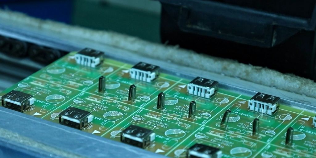
Getting BGA soldering right is a big deal, especially when you’re dealing with sensitive electronics for things like planes or power grids. It’s not just about melting solder; it’s a whole process that needs careful attention at every step. Mess this up, and you’re looking at components that just won’t work or, worse, fail unexpectedly.
Optimizing the Reflow Profile
The reflow oven is where the magic happens, turning solder paste into solid connections. But it’s a delicate dance with temperature. You can’t just blast it with heat. You need a specific temperature curve – a profile – that’s tailored to the solder paste you’re using and the components on the board. This profile usually has a few stages:
- Preheat: This gently raises the temperature across the board to get everything ready and evaporate any leftover solvents in the paste. It helps prevent thermal shock.
- Soak: A period where the temperature stays relatively stable. This allows the entire assembly to reach a uniform temperature, which is key for even melting.
- Peak Reflow: The hottest part, where the solder actually melts and forms those shiny joints. You need to hit the right temperature, but not for too long, or you risk damaging the components or the board.
- Cooling: A controlled cool-down period that solidifies the solder joints without causing stress.
Getting this profile just right means fewer defects like solder balls not melting properly or the board getting warped. It’s all about balance.
Solder Paste Selection for Quality Joints
Choosing the right solder paste is like picking the right glue for a critical job. It’s not one-size-fits-all. You’ve got to think about what the paste is made of, the size of the tiny metal spheres (solder balls) in it, and how the flux (the stuff that helps the solder flow) behaves. For example, in some high-tech areas, lead-free pastes are a must because of environmental rules, but they can sometimes need slightly different handling than older leaded pastes. The goal is to pick a paste that will give you strong, reliable connections without causing problems like solder balls sticking where they shouldn’t or not enough solder making a weak joint.
Design for Manufacturability in BGA Layout
This is about thinking ahead, right from the design stage. How you lay out the pads on the circuit board for the BGA component matters a lot. You need to make sure the pads are the right size and spaced correctly so that when the solder paste is applied and the component is placed, everything lines up perfectly. If the pads are too small, you might not get enough solder. If they’re too big or too close together, you could end up with solder bridges, which are basically unwanted connections between pads. Good design here makes the whole soldering process much smoother and reduces the chances of needing to fix mistakes later.
Challenges and Solutions in BGA Assembly
Alright, so we’ve talked about how great BGA is, but let’s get real for a second. Putting these things together isn’t always a walk in the park. There are definitely some tricky bits that can make you pull your hair out if you’re not careful.
Addressing Rework and Repair Complexities
One of the biggest headaches with BGAs is when something goes wrong and you need to fix it. Because all those little solder balls are hidden underneath the chip, you can’t just look at them to see if they’re good. If a component is faulty or placed incorrectly, taking it off and putting a new one on is a whole production. You need special gear, like rework stations that can heat things up just right without cooking the rest of the board. Plus, you need someone who really knows what they’re doing. Getting this wrong can easily damage the board or nearby parts. It’s not like swapping out a regular chip; it’s a much more involved process.
Overcoming Inspection Difficulties
Following on from the rework issue, checking if the solder joints are actually good is also tough. Like I said, you can’t see them. So, just looking with your eyes isn’t going to cut it. We have to use fancier methods. X-ray machines are pretty common for this, letting us peek inside the solder joints to spot things like air bubbles (voids) or if there wasn’t enough solder. Automated Optical Inspection (AOI) machines can also help, but they sometimes miss things hidden under the package. It’s a bit of a cat-and-mouse game to make sure everything is connected properly. Getting the solder mask thickness right during the PCB design phase is also super important here to avoid issues later on.
Mitigating Misalignment Issues
Then there’s the placement itself. When the BGA chip is being put onto the board, it has to line up perfectly. Even a tiny bit off, and you can end up with bad connections or, worse, no connection at all. Modern machines are pretty good at this, but you still have to be super careful with the setup. Things like making sure the solder paste is applied evenly and the pick-and-place machine is calibrated correctly are key. If the stencil for applying solder paste isn’t aligned right, or if the component shifts even a little during placement, you’re asking for trouble. It’s all about precision.
Applications of Chip BGA Technology
Ball Grid Array (BGA) technology isn’t just a fancy way to connect chips; it’s become a workhorse across so many different industries because it just plain works well. Think about it: we need more power in smaller packages, and BGA helps make that happen. It’s pretty neat how these little solder balls can handle so much.
BGA in Aerospace and Defense
When you’re talking about planes, satellites, or military gear, things have to be tough. Really tough. BGAs are a good fit here because they can handle the shakes, the extreme temperatures, and all the other rough stuff these systems go through. Plus, making things smaller is always a win when you’re trying to fit a lot of tech into a tight space, like in a fighter jet’s cockpit or a satellite’s control system. The reliability is key; you can’t have your navigation system glitching out miles up in the air or in the middle of nowhere.
Energy Sector Applications for BGA
In the energy world, whether it’s power plants, oil rigs, or solar farms, the equipment often operates in some pretty harsh conditions. BGAs help here too. They can handle higher power levels and are built to last in environments that might have moisture or extreme heat. This means the control systems for a wind turbine out at sea or the monitoring equipment for a remote power substation can keep running without a hitch. It’s all about making sure the lights stay on and the systems that manage our energy are dependable.
High-Speed Communication Systems
This is where BGAs really shine. Think about the internet, your phone calls, or data centers – all that stuff relies on moving information super fast. BGAs, especially the newer types like Micro-BGAs, have a tighter spacing between their solder balls. This shorter distance means signals don’t get messed up as they travel, which is a big deal when you’re dealing with gigabits of data per second. They’re used in things like network routers, switches, and the gear that makes our mobile networks tick.
Mobile Devices and Consumer Electronics
This is probably where most of us see BGAs every day, even if we don’t realize it. Your smartphone, your laptop, your gaming console – they all pack a ton of processing power and features into a small, portable package. BGAs are a big reason why this is possible. They allow manufacturers to put more powerful chips closer together on the circuit board, which helps keep devices thin and light. Plus, they help manage the heat generated by these powerful chips, so your phone doesn’t get too hot to hold. It’s a balancing act, and BGAs help get it right.
Wrapping Up: The BGA Advantage
So, we’ve covered a lot about Ball Grid Array technology, from what it is to why it’s so important, especially in tough places like aerospace and energy. It’s clear that getting BGA soldering right, whether it’s the basic stuff or the more advanced micro-BGAs, really matters for making reliable electronics. Keeping up with new methods, like using robots or smarter materials, will be key for companies wanting to stay ahead. By always looking for ways to do things better and trying out new tech, businesses can meet the tough demands of these critical industries. If you need help with BGA soldering, check out what we offer and the industries we work with. Get in touch!
Frequently Asked Questions
What exactly is a Ball Grid Array (BGA) chip?
Think of a Ball Grid Array (BGA) as a special way to connect computer chips to circuit boards. Instead of having little legs like older chips, BGAs have tiny balls of solder underneath them. These balls melt and connect the chip to the board, like a bunch of tiny, neat connections all at once.
Why are BGAs so common in today’s electronics?
BGAs are super important because they let us pack more powerful chips into smaller spaces. They make connections more reliable and help chips run cooler, which is needed for things like smartphones, powerful computers, and even equipment in planes and power plants.
What makes BGA packaging better than older types?
BGAs have several cool benefits! They allow for way more connections in a small area, which means more features in your gadgets. They also help signals travel faster and more cleanly, and they’re better at getting rid of heat, keeping the chip from getting too hot.
What is ‘Flip Chip’ technology in BGA?
When you put a BGA chip on a board, it’s like placing it upside down and connecting it directly. This is called ‘flip chip’ technology. It’s used when you need the absolute best performance, both for speed and for handling heat, because the connections are shorter and more direct.
Why is fixing or replacing BGA chips difficult?
Fixing BGA chips can be tricky because you can’t easily see the solder balls underneath. Special tools and techniques, like using a hot air rework station and X-rays to see the connections, are needed to carefully remove and replace a bad chip without harming the board or other parts.
How do you check if a BGA connection is good?
Because the solder balls are hidden under the chip, you can’t just look at them to see if the connection is good. Special tools like X-ray machines are used to check if the solder joints are properly made, making sure there are no hidden problems.