So, you’re looking into how chips get put together, huh? It’s not just about the silicon itself; the way it’s packaged is a pretty big deal. Think of it like building a house – you need a solid foundation and good walls, not just fancy furniture inside. This whole ic packaging design thing has really changed over the years. It used to be simple, but now it’s way more complicated and important for making our gadgets work well. We’re going to break down what goes into it, from the basics to some pretty advanced stuff.
Key Takeaways
- The way a chip is packaged is just as important as the chip itself for how well a device performs. Good ic packaging design can make a big difference.
- There are many different ways to package chips, and the best choice depends on what the device needs to do, how much it should cost, and how many will be made.
- Putting different kinds of chips together in one package, often called chiplets, is a major trend that lets us build more powerful and smaller electronics.
- Making sure the package can handle heat and send signals without problems is a big part of the design process, affecting reliability.
- The process of designing and making these packages involves many steps, from preparing the wafer to the final assembly, and it’s important to think about the whole supply chain.
Fundamentals Of IC Packaging Design
Understanding The Importance Of IC Packaging
So, you’re building some cool new electronic gadget, right? You’ve probably spent ages thinking about the processor, the memory, all that fancy silicon. But what about how it all gets put together? That’s where IC packaging comes in, and honestly, it’s way more important than a lot of people give it credit for. Think of it like the foundation and walls of a house – without them, the roof (the chip) doesn’t do much good. Packaging isn’t just about sticking a chip in a plastic box to keep it safe. It’s a whole engineering discipline that can actually make your device faster, smaller, and use less power. Seriously, the way a chip is packaged can totally change how well it performs in the real world. The market for this stuff is huge, too – billions of dollars are spent every year, and it’s growing. This tells you that companies are realizing packaging isn’t just an afterthought; it’s a key part of making their products work well and stand out.
Key Technical Specifications And Parameters
When you start looking at different ways to package an integrated circuit (IC), you’ll run into a bunch of technical terms. It can seem like a lot at first, but knowing these helps you pick the right one. Here are some of the big ones:
- Pin Count: This is just the number of connections the package has to the outside world, like the pins on a chip. Some have just a few, others have thousands.
- Pitch: This is the spacing between those pins or balls. Smaller pitch means you can fit more connections into a smaller area, which is great for making things tiny.
- Form Factor: Basically, the size and shape of the package itself. Does it need to be super thin for a smartphone, or can it be a bit chunkier?
- Thermal Performance: How well does the package get rid of heat? This is often measured as thermal resistance. If a chip gets too hot, it won’t work right, or it might even break.
- Electrical Performance: This covers things like how signals travel in and out, looking at things like inductance and capacitance. Good electrical performance means less interference and faster signals.
- Reliability Metrics: This is about how tough the package is. Can it handle temperature changes? How does it react to moisture? Can it survive being dropped?
Getting these specs right is pretty important for making sure your chip does what you want it to do, without overheating or failing.
Evolution From Basic To Advanced Architectures
IC packaging hasn’t always been this complicated. Back in the day, like the 1960s, packages were pretty simple. You had things like Dual In-line Packages (DIPs), which were these chunky plastic or ceramic blocks with two rows of pins sticking out. They did the job of protecting the chip and connecting it, but that was about it.
But as chips got more powerful and people wanted smaller gadgets, packaging had to change. We saw moves towards:
- Surface Mount Technology (SMT): Packages that could be soldered directly onto the surface of a circuit board, instead of needing to be pushed through holes. This made assembly faster and allowed for denser boards.
- Ball Grid Arrays (BGAs): Instead of pins, these use little solder balls on the bottom. This lets you have way more connections in a smaller space and generally offers better thermal performance.
- Flip Chip: Here, the chip is flipped upside down and connected directly to the package substrate using tiny bumps. This shortens the electrical path, improving performance.
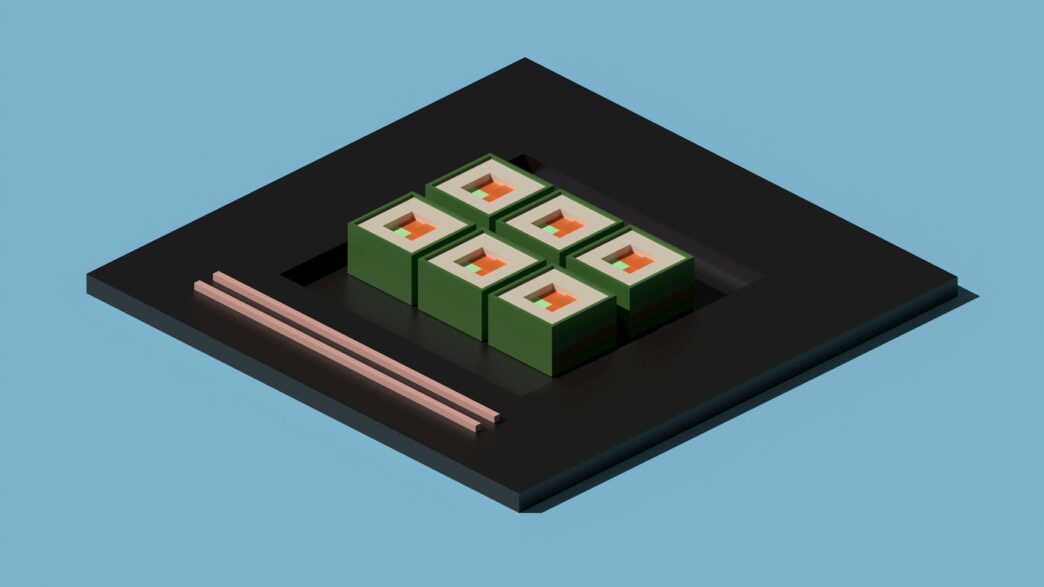
And it didn’t stop there. Now we’re seeing even more complex stuff like stacking multiple chips on top of each other (3D packaging) or mixing different types of chips together (heterogeneous integration). It’s a constant race to pack more power and features into smaller spaces, and packaging is right at the heart of it.
Exploring Advanced IC Packaging Technologies
So, we’ve covered the basics, but the real magic happens when we start talking about advanced IC packaging. This isn’t just about putting a chip in a box anymore; it’s about cleverly combining multiple chips and components to create something much more powerful and compact than a single, giant chip could ever be. Think of it like building with LEGOs instead of trying to sculpt a whole statue from one giant block of marble. It opens up a whole new world of possibilities for performance and size.
Heterogeneous Integration And Chiplets
This is a big one. Heterogeneous integration means mixing and matching different types of chips – like a CPU, a GPU, memory, and maybe even some specialized AI accelerators – all within the same package. Instead of trying to build one massive, complex chip (which gets really hard and expensive), we break it down into smaller, specialized pieces called chiplets. These chiplets are then assembled together. It’s like having a team of specialists, each doing their best job, rather than one person trying to do everything poorly.
- Benefits of Chiplets:
- Better Yields: If one small chiplet fails during manufacturing, you only lose that one, not the entire massive chip.
- Cost Savings: You can use the best manufacturing process for each type of chiplet, which is often cheaper than a one-size-fits-all approach.
- Faster Time-to-Market: Companies can reuse existing chiplets or quickly develop new ones without redesigning everything from scratch.
- Customization: You can mix and match chiplets to create custom solutions for specific needs.
2.5D And 3D Packaging Approaches
These are ways to physically arrange those chiplets or multiple dies.
- 2.5D Packaging: Imagine laying out your chiplets side-by-side on a special silicon bridge, called an interposer. This interposer has tiny wires running through it to connect all the chips. It’s "2.5D" because the chips are on the same plane, but the interposer adds a layer of complexity and connection capability. This is great for high-speed communication between chips.
- 3D Packaging: This is where things get stacked. We’re talking about putting chips directly on top of each other, connected by tiny vertical pathways called Through-Silicon Vias (TSVs). This dramatically shrinks the footprint, making devices incredibly small. It also shortens the distance signals have to travel, which can boost performance and power efficiency.
Fan-Out Wafer-Level Packaging
This technique is pretty neat because it allows the package to be bigger than the actual chip itself. After the chip is made, it’s embedded in a molding compound, and then new connections (redistribution layers or RDLs) are built on top. This lets you have way more connection points (I/O) without needing a bigger chip die. It’s especially popular for mobile devices where space is super tight but you still need lots of connections.
System-In-Package Solutions
Think of a System-in-Package (SiP) as a complete mini-system packed into a single enclosure. Instead of just one chip, a SiP can contain multiple chips (like processors, memory, sensors, and other components) that work together. It’s like building a small, self-contained electronic device within the package itself. This approach is fantastic for creating highly integrated products like smartphones, wearables, and advanced automotive electronics where space and functionality are key.
The IC Packaging Design Process
So, you’ve got this amazing chip design, right? It’s all shiny and new, ready to do incredible things. But hold on a sec, that bare silicon wafer isn’t going to magically connect to your circuit board. That’s where the whole packaging design process kicks in. It’s not just about slapping a lid on your chip; it’s a whole strategic phase that can seriously make or break your product. Getting this part right early on saves a ton of headaches later.
Defining Packaging Requirements
First things first, you gotta figure out what your chip actually needs from its package. This isn’t a one-size-fits-all deal. Think about:
- Performance: How fast does this thing need to run? What kind of signals are we talking about? High-speed stuff needs special attention to avoid noise and signal loss.
- Heat: Chips get hot, especially when they’re working hard. The package has to be able to get rid of that heat, or your chip will just throttle down or, worse, fry.
- Size and Shape: Where is this chip going to live? Is it a tiny wearable device, or a big server rack? The physical constraints are super important.
- How Tough Does It Need to Be?: Will it be in a rugged industrial setting, or just sitting on a desk? Reliability is key, and different environments demand different levels of protection.
- How Many Are We Making?: Are you building a few hundred for a niche product, or millions for a consumer gadget? Production volume massively impacts cost and manufacturing choices.
Evaluating Packaging Options
Once you know what you need, it’s time to look at what’s out there. There are a bunch of different ways to package a chip, each with its own pros and cons. It’s like picking the right kind of house for your needs – you wouldn’t build a skyscraper for a single person, right?
Here’s a quick look at some common types and what they’re good for:
| Packaging Type | Typical Use Cases | Key Considerations |
|---|---|---|
| QFP/SOIC | Older consumer electronics, simpler devices | Low cost, easy to assemble, but larger footprint |
| BGA/CSP | Mobile phones, laptops, gaming consoles | Smaller size, better electrical performance, thermal challenges |
| Flip Chip | High-performance CPUs, GPUs, AI accelerators | Direct connection, excellent electrical/thermal, higher cost |
| Fan-Out WLP | Smartphones, wearables, IoT devices | Very small form factor, good performance, complex process |
| 2.5D/3D Stacking | High-end servers, AI, advanced computing | Extreme density, massive performance gains, very high cost |
Risk Assessment and Decision-Making Framework
Okay, so you’ve got a few options that look promising. Now, you need to be a bit of a detective and figure out the potential downsides. Nobody wants surprises down the road.
- Manufacturing Maturity: Is this a brand-new, cutting-edge technique that only a couple of places can do, or is it something well-established with lots of suppliers?
- Supply Chain: Can you actually get these packages reliably? Are there multiple companies that can make them, or are you putting all your eggs in one basket?
- Testing: How are you going to test these things once they’re packaged? Some advanced packages can be tricky to test thoroughly.
- What If It Fails?: What happens if a batch of these packages has issues? How easy is it to figure out what went wrong and fix it?
Total Cost of Ownership Analysis
This is where you look beyond just the price tag of the package itself. You gotta think about the whole picture, from start to finish.
- Development Costs: How much time and money will it take to design and verify the package?
- Tooling and Setup: Are there special machines or molds needed? That can add up fast.
- Assembly Costs: How much does it cost to actually put the chip into the package?
- Testing Costs: As mentioned, testing can be a big expense, especially for complex packages.
- Yield: What percentage of packaged chips are expected to work correctly? Lower yields mean higher costs per working chip.
- Reliability and Warranty: What’s the expected lifespan of the product? If it fails early, you’re looking at warranty claims and unhappy customers. That’s a cost, too.
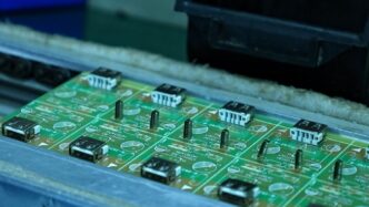
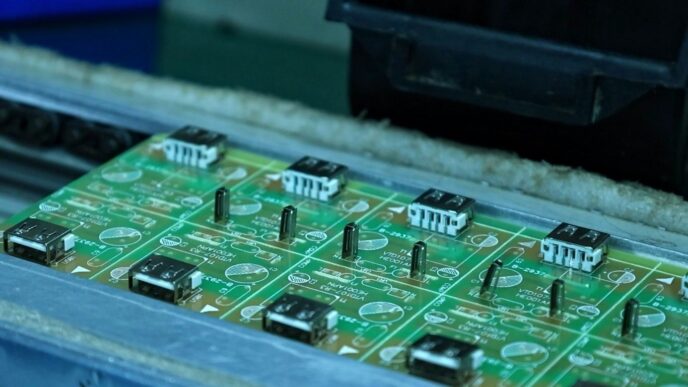
Manufacturing And Assembly Essentials
So, you’ve got your chip design all sorted, but how does it actually get into that little black thing you see on a circuit board? That’s where manufacturing and assembly come in, and honestly, it’s a whole world of its own. It’s not just about slapping things together; there’s a lot of precision involved.
Wafer Preparation And Dicing
First off, you start with a wafer, usually silicon, with tons of identical chips on it. Before you can separate these chips, they need some prep work. This often involves grinding down the wafer to a specific thickness. Then comes dicing, which is basically cutting the wafer into individual chips, called dies. Think of it like cutting a pizza, but way, way more delicate. They use diamond saws or lasers for this, and you have to be super careful not to damage the tiny circuits on each die. It’s a critical step because a bad cut means a bad chip, and nobody wants that.
Wire Bonding And Flip Chip Assembly
Once you have your individual dies, you need to connect them to the outside world. There are a couple of main ways to do this. Wire bonding is a more traditional method where super-fine wires, usually gold or copper, are bonded from the pads on the die to the leads of the package. It’s like creating tiny bridges. Then there’s flip-chip assembly. This is a bit more advanced. The die has tiny bumps on it, and it’s literally flipped over and attached directly to the substrate or package using these bumps. This allows for more connections and better performance, but it’s also more complex to set up.
Wafer-Level Packaging Processes
Sometimes, the packaging happens right on the wafer before it’s even diced. This is called wafer-level packaging (WLP). It’s pretty neat because it can be more cost-effective for high-volume production. Processes like creating redistribution layers (RDLs) and adding solder bumps can all be done while the chips are still on the wafer. This means you’re packaging many chips at once, which can speed things up. It’s a bit like doing all your prep work before you cut up your ingredients for a big meal.
Supply Chain And Facility Considerations
Putting all this together isn’t something you can just do in your garage. You need specialized facilities, clean rooms, and a whole lot of equipment. Plus, there’s the supply chain. You’ve got raw materials, wafer fabrication, assembly houses, testing facilities – it’s a complex network. Making sure all these pieces work together smoothly is just as important as the technical steps themselves. You need reliable partners and a well-managed process to get your chips from silicon to a finished product that actually works.
Ensuring Reliability In IC Packaging
So, we’ve talked about how to design these fancy packages, but what happens when things get tough? That’s where reliability comes in. It’s not just about making a chip work; it’s about making sure it keeps working, no matter what.
Thermal Management Strategies
Chips get hot. Like, really hot sometimes. If you don’t get that heat away, things start to break down. It’s like trying to run a marathon in a sauna – not ideal.
- Heat Sinks: These are those metal things you often see attached to processors. They have a lot of surface area to help spread the heat out.
- Thermal Interface Materials (TIMs): Think of these as special pastes or pads that fill in tiny gaps between the chip and its cooling solution. They make sure heat can transfer smoothly.
- Heat Pipes: These are pretty neat. They use a liquid that evaporates and condenses to move heat away from the chip very efficiently.
- Fan-Out Wafer-Level Packaging: This approach can actually help with heat dissipation by spreading the heat over a larger area before it even gets to the main board.
Signal Integrity and Power Delivery
This is about making sure the electrical signals going to and from the chip are clean and that the chip gets the power it needs without any hiccups. Imagine trying to have a conversation in a noisy room – it’s hard to hear what’s being said. Bad signal integrity is like that for electronics.
- Controlled Impedance: This means designing the pathways for signals so they have a consistent electrical resistance. It helps prevent signals from bouncing back or getting distorted.
- Decoupling Capacitors: These are like tiny, fast batteries placed near the chip. They can quickly supply extra power when the chip needs a sudden burst, smoothing out the power delivery.
- Ground Planes: Having a solid ground plane on the circuit board helps shield signals from interference and provides a stable reference for everything.
Failure Analysis and Reliability Testing
Okay, so we’ve designed it to be tough, but how do we know it’s tough? We test it. And if something does go wrong, we figure out why.
- Temperature Cycling: We put the package through repeated cycles of hot and cold to see if it can handle the expansion and contraction without cracking.
- Humidity Testing: We expose it to high humidity and heat to check for moisture-related failures, like corrosion.
- Mechanical Stress Tests: This includes things like dropping the device (within reason!) or applying pressure to see how it holds up.
- Failure Analysis: When a part fails, we use fancy microscopes and tools to pinpoint the exact cause. This feedback is super important for improving future designs. You can find more details on reliability testing methods in industry reports.
Package Durability and Improvement
Ultimately, we want these packages to last. It’s not just about passing tests; it’s about making sure the product works reliably for its intended lifespan. This often involves looking at the materials used, the assembly processes, and even how the end-user interacts with the device. Continuous improvement is key here. We learn from testing, from field data, and from new material science to make the next generation even better. It’s a cycle of design, test, learn, and repeat.
Future Trends In IC Packaging Design
So, what’s next for IC packaging? It feels like things are moving faster than ever, and honestly, it’s pretty exciting. We’re seeing a big shift away from just making bigger chips and more towards clever ways of putting smaller, specialized pieces together.
Chiplet-Based Modular Designs
This is a pretty huge deal. Instead of one giant, complex chip, designers are breaking things down into smaller, independent "chiplets." Think of it like building with LEGOs. Each chiplet can be optimized for a specific job – one for processing, another for memory, maybe a third for graphics. Then, they’re all put together in a single package. This approach offers a lot of flexibility. You can mix and match chiplets from different manufacturers, which could speed up development and potentially lower costs. Plus, if one chiplet has a defect, you don’t necessarily have to scrap the whole thing; you might just replace that one piece. It’s all about modularity and customization.
Advanced Interconnect Technologies
Putting all these chiplets together requires some serious connection tech. We’re talking about things like 2.5D and 3D stacking, where chips are placed side-by-side on an interposer or stacked directly on top of each other. This allows for much shorter distances between the chips, which means faster communication and less power used. It’s like upgrading from a country road to a superhighway for data. Technologies like through-silicon vias (TSVs) are key here, acting like tiny vertical tunnels to connect stacked layers. The goal is to pack more functionality into a smaller space with better performance.
Emerging Packaging Materials
Beyond just the structure, the materials used in packaging are also getting a makeover. We’re seeing research into new polymers, ceramics, and even composites that can handle higher temperatures, offer better electrical insulation, or provide improved thermal dissipation. Some materials might be lighter, which is a big deal for portable devices. Others could be more robust, making electronics last longer in tough environments. It’s a constant search for materials that can keep up with the demands of next-gen chips.
Sustainability In Packaging
This is becoming a bigger topic, and rightly so. As we use more electronics, we need to think about the environmental impact. This means looking at packaging that uses less material, is easier to recycle, or is made from more sustainable sources. Companies are exploring ways to reduce waste during manufacturing and to design packages that have a longer lifespan, reducing the need for frequent replacements. It’s about making our tech footprint a little lighter on the planet.
Wrapping It Up
So, we’ve gone through a lot, from the basic ideas behind putting chips into packages to some pretty advanced stuff. It’s clear that packaging isn’t just an afterthought anymore; it’s a big deal in how well electronics work. Choosing the right package can really make or break a product. As things keep changing fast, staying on top of these packaging techniques is key. Keep learning, keep experimenting, and remember that smart packaging design is a major part of making great tech.
Frequently Asked Questions
What exactly is IC packaging and why is it so important?
Think of IC packaging like a protective case for a tiny computer chip. It’s super important because it not only keeps the delicate chip safe from damage, but it also helps it connect to other parts of an electronic device, like your phone or computer. Good packaging makes the chip work better and last longer.
How has IC packaging changed over time?
It’s changed a lot! In the past, packages were pretty basic, just simple boxes to hold chips. Now, we have really fancy ways to stack chips on top of each other or put different types of chips together in one package. This allows us to make devices much smaller and more powerful.
What are chiplets and heterogeneous integration?
Chiplets are like smaller, specialized chips that can be combined to create a bigger, more powerful system. Heterogeneous integration is the fancy term for putting these different chiplets together in a single package. It’s like building with LEGOs instead of trying to carve a whole model out of one big block of wood.
What’s the difference between 2.5D and 3D packaging?
In 2.5D packaging, chips are placed side-by-side on a special platform called an interposer, which helps them talk to each other faster. In 3D packaging, chips are stacked directly on top of each other, which saves even more space and can make them work together more efficiently.
How do companies decide which type of IC packaging to use?
It’s a bit like choosing the right tool for a job. Companies look at what the chip needs to do (like how fast it needs to be or how much heat it makes), how many they need to make, and how much they can spend. They also think about making sure the package will last a long time without breaking.
What are some new ideas for IC packaging in the future?
We’re going to see even more use of chiplets to build custom systems. Also, new materials are being explored to help chips run cooler and faster. There’s also a growing focus on making the packaging process more eco-friendly, using less energy and materials.