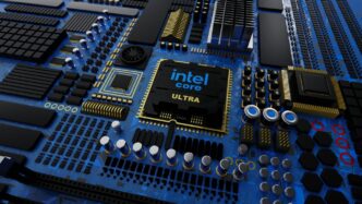

You know, we talk a lot about the fancy chips inside our phones and computers, but what about the stuff that holds them all together? It’s easy to forget about the integrated circuit packaging, but honestly, it’s a pretty big deal. Think of it as the chip’s bodyguard and its connection to the outside world. Without good packaging, even the smartest chip wouldn’t work right, or it might break easily. This packaging stuff has really changed over the years, and it’s what lets us have all these tiny, powerful gadgets we use every day. Let’s look at why this often-overlooked part of electronics is so important.
Key Takeaways
- Integrated circuit packaging does more than just protect chips; it’s vital for making sure they work correctly and connect to everything else.
- Older methods like wire-bonding are still around, but newer techniques like flip-chip and system-in-package are needed for better performance and smaller sizes.
- Advanced packaging, like 2.5D and 3D stacking, helps make electronics smaller and more powerful, especially for things like AI and high-performance computers.
- The materials used in packaging, from heat-dissipating compounds to special substrates, play a big role in how well a chip performs and lasts.
- Packaging is key to making devices smaller, improving their reliability in tough situations, and enabling complex technologies like AI and self-driving cars.
The Foundational Purpose of Integrated Circuit Packaging
Think of an integrated circuit, or IC, as the brain of your electronic gadget. It’s a tiny piece of silicon packed with billions of transistors, doing all the heavy lifting. But this brain is delicate. It can’t just sit out in the open. That’s where packaging comes in. It’s not just a fancy case; it’s a critical part of the whole system, acting as the go-between for the chip and everything else.
Protection From Environmental Factors
ICs are sensitive. Dust, moisture, and even physical bumps can cause serious problems, leading to malfunctions or outright failure. Packaging acts as a shield, keeping these delicate components safe from the outside world. It’s like putting a helmet on your brain – it protects it from impacts and the elements.
Ensuring Electrical Connectivity and Signal Integrity
Beyond just protection, the package is responsible for connecting the chip to the rest of the circuit board. This involves tiny wires or solder bumps that carry electrical signals. The way these connections are made directly impacts how fast and accurately signals travel. Poor connections can lead to dropped signals or distorted information, slowing down your device or making it unreliable. Good packaging means clean, direct pathways for those signals to do their job without getting messed up.
Thermal Management for Optimal Performance
When an IC works hard, it generates heat. Too much heat is bad news for electronics; it can slow down performance and shorten the lifespan of the chip. Packaging plays a big role in getting rid of this heat. It often includes materials and designs that help spread the heat out and away from the chip, keeping it cool enough to operate at its best. It’s like a tiny radiator for the chip.
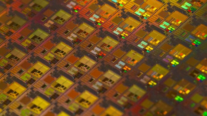
Evolution of Semiconductor Packaging Techniques
So, we’ve talked about why chips need packaging in the first place. Now, let’s look at how we got here. Semiconductor packaging has really changed over the years, moving from just keeping things safe to actually making chips work better. It’s kind of like how phone cases went from basic bumpers to fancy multi-tools.
Wire-Bond Technology: A Legacy Method
This is one of the oldest tricks in the book for connecting a chip to its package. Basically, tiny wires, usually gold or copper, are used to link the pads on the chip to the pins on the package. It’s been around forever because it’s pretty reliable and doesn’t cost a fortune. Think of it as the dependable, old-school way of doing things. It’s still used a lot, especially for chips that don’t need to be super-fast or incredibly small. It’s a solid choice for many applications, but it does have its limits when you start pushing for more performance.
Flip-Chip Integration for Enhanced Performance
Things got more interesting with flip-chip. Instead of wires going up and over, the chip is flipped upside down, and tiny solder bumps directly connect the chip to the package substrate. This means shorter connections, which translates to faster signals and less interference. It’s a big step up from wire bonding, allowing for more connections and better electrical performance. This method is great for chips that need to handle a lot of data quickly, like processors in your computer or graphics cards. It really helped pave the way for more powerful electronics.
System-in-Package for Multifunctional Devices
Then came the idea of putting multiple chips, or different types of chips, all into one package. This is System-in-Package, or SiP. Instead of having separate chips for, say, your phone’s processor, memory, and radio, you can combine them. This makes the whole thing smaller and can sometimes be cheaper than making one giant, super-complex chip. It’s a smart way to pack a lot of functionality into a small space, which is exactly what we need for all those gadgets we carry around. It’s a key part of how we get so much power in such small devices today, and you can see it in action in many consumer electronics.
These techniques show how packaging isn’t just an afterthought; it’s a core part of how we design and build electronics. Each method has its place, and understanding them helps us appreciate the complexity behind the devices we use every day.
Advanced Integrated Circuit Packaging Solutions
Okay, so we’ve talked about the basics, but things get really interesting when we look at the cutting-edge stuff in IC packaging. These aren’t your grandpa’s circuit boards anymore. We’re talking about ways to cram more power and functionality into smaller spaces, which is pretty wild when you think about it.
2.5D and 3D Packaging for Miniaturization
This is where things get stacked, literally. Instead of laying chips out flat, we’re stacking them on top of each other. Think of it like building a skyscraper for electronics instead of a sprawling ranch house. This vertical approach saves a ton of space, which is a big deal for everything from your smartphone to supercomputers. 2.5D and 3D packaging allow us to pack more processing power into a smaller footprint than ever before. It’s not just about making things smaller, though; it also helps speed things up and use less power because the signals don’t have to travel as far.
Heterogeneous Integration for Diverse Components
This is kind of like a "mix and match" approach. Instead of putting only one type of chip in a package, we can now combine different kinds of chips – like logic, memory, and even specialized chips for things like AI – all into one single package. It’s a way to build really specialized devices without having to design a whole new monolithic chip. This is super useful for things like advanced AI processors or the gear needed for 5G.
Wafer-Level Packaging Innovations
This is a bit different. Instead of packaging chips one by one after they’re cut from the silicon wafer, wafer-level packaging (WLP) does the packaging steps while the chips are still on the wafer. It’s like decorating the whole sheet of cookies before you cut them out. This can save a lot of time and money, and it also results in some of the smallest packages you can get. These are great for tiny devices like wearables or the sensors in your smart home gadgets.
Materials Driving Packaging Advancements
You know, it’s easy to get caught up in the shiny new chips and processors, but what’s holding all that magic together? The materials used in integrated circuit (IC) packaging are seriously important. They’re not just filler; they’re key players in how well a chip performs and how long it lasts. Think of them as the unsung heroes.
High-Performance Thermal Interface Materials
Chips get hot. Like, really hot, especially when they’re working hard on complex tasks. If that heat can’t escape, the chip can slow down or even get damaged. That’s where thermal interface materials (TIMs) come in. These materials sit between the chip and its heat sink, making sure heat moves away efficiently. We’re talking about stuff like specialized pastes, pads, and even liquids that are way better at conducting heat than air. Getting the right TIM is critical for keeping high-performance chips from overheating.
Low-k Dielectrics and Conductive Adhesives
When signals zip around inside a chip, they can interfere with each other. Low-k dielectrics are materials that have a low dielectric constant, meaning they don’t let electrical fields pass through easily. This helps reduce unwanted capacitance between wires, allowing signals to travel faster and with less noise. It’s a big deal for high-speed electronics. Then there are conductive adhesives. Instead of traditional wire bonds, these glues can actually conduct electricity. They’re lighter, smaller, and can offer better electrical connections for certain applications, especially when you’re trying to pack a lot into a small space. These are becoming more common in advanced packaging, helping to shrink down devices like smartphones and wearables.
Advanced Substrates and Interposers
The base layer that holds the chip and connects it to the rest of the circuit board is called a substrate. Traditionally, these were often made of fiberglass-like materials. But now, we’re seeing more advanced substrates, including ones made from silicon or even glass. These materials can handle much finer wiring and offer better electrical performance. Interposers, which are like super-precise bridges, are also gaining traction. They allow multiple chips, or ‘chiplets’, to be connected very closely together, almost like they’re one big chip. This is a big part of how we’re getting more power into smaller packages, enabling things like next-generation devices.
Here’s a quick look at some material types and their roles:
- Plastics: Still widely used for their low cost and good insulation, especially in standard IC packages.
- Ceramics: Offer great heat and electrical properties, good for demanding applications but pricier.
- Silicon/Glass: Used for advanced substrates and interposers, providing superior electrical performance and finer interconnects.
- Thermal Interface Materials (TIMs): Pastes, pads, and liquids designed to move heat away from the chip.
- Low-k Dielectrics: Reduce signal interference for faster, cleaner signals.
- Conductive Adhesives: Replace wire bonds for smaller, lighter connections.
The Impact of Packaging on Modern Electronics
You know, we spend a lot of time talking about the chips themselves – the brains of our gadgets. But honestly, the packaging they live in? It’s a pretty big deal, and maybe we don’t give it enough credit. Think of it like the house for your computer’s brain. A fancy brain in a leaky, cramped house isn’t going to do much good, right?
Enabling Miniaturization in Consumer Devices
This is where packaging really shines for the stuff we use every day. Remember when phones were chunky bricks? Packaging advancements have been a huge part of shrinking all that tech down. We’re talking about fitting more and more power into smaller spaces, which is why your smartphone can do more than a desktop computer from just a decade ago. It’s not just about making things smaller, though. It’s about making them work better in that small space.
- Smaller footprints: Advanced packaging allows multiple components to be stacked or placed very close together, reducing the overall size of the electronic module.
- Improved power efficiency: Shorter connections within the package mean less energy is wasted, leading to longer battery life in portable devices.
- Better thermal management: As components get packed tighter, heat becomes a bigger problem. New packaging materials and designs help get that heat away, so your phone doesn’t overheat when you’re playing a game.
Supporting High-Performance Computing and AI
For the really heavy-duty stuff, like supercomputers or the processors crunching numbers for artificial intelligence, packaging is absolutely critical. These chips work incredibly hard and generate a ton of heat. If that heat isn’t managed, performance tanks, and the chips can even get damaged. Advanced packaging techniques are what allow these powerful systems to run at their best.
- Higher data throughput: Techniques like 2.5D and 3D integration allow for more connections between different chips (like processors and memory) in a single package, speeding up how fast data can move.
- Efficient heat dissipation: Specialized materials and structures within the package are designed to pull heat away from the hot silicon, keeping performance stable even under heavy loads.
- Integration of diverse functions: Heterogeneous integration lets designers combine different types of chips – say, a CPU, a GPU, and memory – into one package. This is a game-changer for AI, where different tasks need different kinds of processing power.
Enhancing Reliability in Critical Applications
When electronics are used in places where failure just isn’t an option – think medical devices, airplanes, or cars – the packaging has to be top-notch. It’s not just about performance; it’s about making sure the chip can handle tough conditions and keep working for a long time. The right packaging acts as a robust shield against environmental hazards and physical stress.
Here’s a look at what makes packaging so important for reliability:
- Environmental Protection: Packaging shields the delicate silicon from moisture, dust, chemicals, and even radiation, which can cause malfunctions.
- Mechanical Strength: It provides a sturdy structure that can withstand vibrations, shocks, and the stresses of assembly and operation.
- Thermal Stability: By managing temperature fluctuations, packaging prevents components from overheating or experiencing thermal cycling damage, which can lead to cracks or failures over time.
Future Trajectories in Integrated Circuit Packaging
So, what’s next for how we wrap up these tiny electronic brains? It turns out, the world of chip packaging is far from settled. We’re seeing some really interesting shifts happening, driven by the need for smaller, faster, and more efficient electronics. It’s not just about making things smaller anymore; it’s about making them smarter and more sustainable too.
Sustainability and Eco-Friendly Solutions
Let’s face it, electronics generate waste, and the industry is starting to take notice. There’s a big push towards making packaging greener. This means looking at ways to cut down on hazardous materials, use more recyclable stuff, and even explore biodegradable options. Think less lead in solder and more plant-based plastics. It’s a slow process, but companies are realizing that being environmentally conscious can also be a good business move. It’s about building a cleaner supply chain for the future.
AI-Driven Design and Manufacturing Automation
As chip packages get more complicated, trying to design them by hand is becoming a real headache. That’s where artificial intelligence comes in. AI and machine learning are being used to figure out the best layouts, pick the right materials, and even optimize how the chips are made. This speeds things up a lot, cutting down development time and helping to reduce errors. It means we can get new, cutting-edge products out the door much faster.
The Growing Importance of 3D Packaging
This is a big one. 3D packaging is really set to take over because it lets us pack more power into a smaller space. By stacking chips on top of each other and connecting them with tiny vertical pathways, we get incredible power efficiency and performance boosts. This is especially important for things like AI accelerators and high-performance computing. While managing the heat and the cost of making these stacked chips are still challenges, the potential for next-generation integrated circuits is huge. It’s a complex but very promising area for the future of electronics.
Wrapping It Up
So, we’ve talked a lot about how integrated circuit packaging isn’t just some boring box around a chip. It’s actually a pretty big deal for how our gadgets work, how long they last, and how small they can get. From protecting the delicate insides to helping chips talk to each other faster, packaging is doing a lot of heavy lifting. As technology keeps moving forward with things like AI and super-fast internet, the way we package these chips is going to change even more. It’s kind of amazing to think that something so small can have such a huge impact on the electronics we use every single day. It’s definitely a field worth keeping an eye on.
Frequently Asked Questions
What is the main job of a chip package?
Think of a chip package like a protective case for a tiny computer chip. Its main jobs are to keep the chip safe from bumps, dust, and moisture, and to connect it so it can talk to the rest of your electronic device. It also helps keep the chip from getting too hot.
Why are there different ways to package chips?
Different chips have different needs! Some need to be super fast, others need to handle a lot of power, and some need to fit into really small spaces. So, engineers have come up with various packaging methods, like older wire-bonding techniques and newer flip-chip or 3D methods, to make sure each chip works its best for its specific job.
What does ‘heterogeneous integration’ mean for chip packaging?
Heterogeneous integration is like putting different kinds of puzzle pieces together in one box. It means packing different types of chips, like processors and memory chips, into a single package. This allows them to work together more closely and efficiently, making devices like smartphones and AI computers much more powerful.
How does packaging help make electronics smaller?
Packaging is a big help in making gadgets smaller! Advanced packaging lets engineers stack chips on top of each other (like in 3D packaging) or pack them very tightly together. This means you can fit more computing power into a smaller space, which is why our phones and smartwatches keep getting thinner and lighter.
Are there new materials being used in chip packaging?
Yes, definitely! Scientists are developing special materials to help chips run cooler, send signals faster, and last longer. This includes things like special pastes that move heat away from the chip and new types of base materials that help signals travel more smoothly.
What’s next for chip packaging?
The future is exciting! We’ll see more focus on making packaging environmentally friendly, using smart computers (AI) to design them better and faster, and continuing to stack chips in 3D to make electronics even more powerful and compact. The goal is to make chips work better while being kinder to the planet.