So, you’ve probably heard the term “flip chip IC” floating around, especially if you’re into electronics. It’s a pretty big deal in how we make computer chips and other electronic bits work better and smaller. Basically, it’s a way to connect the chip to the board that’s different from the old-school methods. This technology is showing up in everything from your phone to super-fast computers, and it’s changing how we design and build electronics. Let’s break down what this flip chip IC stuff is all about.
Key Takeaways
- Flip chip IC technology connects chips directly to a substrate using tiny solder bumps, ditching the wires used in older methods.
- This direct connection means signals travel faster and heat can escape more easily, making devices perform better.
- The flip chip IC approach allows for way more connections (I/O) in a smaller space, leading to smaller and more powerful gadgets.
- Key steps in making a flip chip IC package include preparing the bumps on the chip, aligning it to the substrate, melting the bumps to create connections, and adding a protective material.
- Flip chip IC is used everywhere, from high-performance computers and smartphones to power electronics and advanced systems that combine multiple chips.
Understanding Flip Chip IC Technology
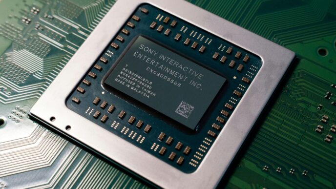
So, what exactly is this ‘flip chip’ thing everyone’s talking about in the world of integrated circuits? Basically, it’s a way to package chips that’s pretty different from the old-school methods. Instead of connecting wires to the top of the chip, you flip the chip over – hence the name – and connect it directly to the circuit board using tiny little bumps. This direct connection is the key to a lot of its benefits.
The Evolution of Flip Chip IC Substrate
This isn’t some brand-new idea that just popped up. People were tinkering with flip chip concepts way back in the 1960s. But it really started to take off in the 1990s, mostly because our electronic gadgets started getting smaller and needing to do way more, way faster. Think about how much phones and computers have changed since then. Flip chip technology was right there, powering that evolution.
Core Concepts of Flip Chip IC Packaging
At its heart, flip chip packaging is about making connections differently. Imagine a regular chip; it has connection points, usually on the edges. With flip chip, you put little solder bumps on those connection points. Then, you flip the chip over so the bumps face down and connect directly to a substrate. This is a big change from wire bonding, where fine wires connect the chip to the substrate.
Here’s a quick look at the main differences:
- Connection Method: Flip chip uses solder bumps for direct connection. Wire bonding uses thin wires.
- Orientation: Flip chip has the active side facing down. Wire bonding has the active side facing up.
- Connection Area: Flip chip connects across the entire surface of the chip. Wire bonding typically connects around the perimeter.
Flip Chip IC vs. Traditional Wire Bonding
Why bother with flip chip when wire bonding has been around forever? Well, flip chip offers some pretty significant advantages, especially as electronics get more demanding. The biggest win is performance. Because the connections are so much shorter – no long wires to travel – signals move faster and with less interference. Plus, those bumps can handle more current and dissipate heat better than wires. This means chips can run faster and hotter without melting down.
- Electrical Performance: Shorter paths mean less delay and noise.
- Thermal Performance: Larger contact area helps move heat away more effectively.
- I/O Density: Connecting across the whole chip surface allows for many more connections, which is vital for complex processors.
Key Advantages of Flip Chip IC Integration
So, why are we even bothering with flip chip technology? It’s not just some fancy new way to stick chips together; it actually brings some pretty big benefits to the table, especially when you compare it to older methods like wire bonding. Think of it like upgrading from a dial-up modem to fiber optics – the difference is huge.
Enhanced Electrical Performance
This is probably the biggest win for flip chip. Because the chip is flipped over and connected directly to the substrate with tiny bumps, the wires are super short. This means signals travel faster and with less interference. Less signal delay and less power wasted? Yes, please. For high-speed stuff, this is a game-changer. It’s like having a direct highway for your data instead of a winding country road.
Superior Thermal Dissipation
Modern electronics get hot. Like, really hot. Flip chip helps manage that heat much better than wire bonding. The direct connection from the chip to the substrate acts like a more efficient heat sink. This means chips can run harder for longer without overheating and failing. Some reports suggest flip chip packages can handle power densities way higher than traditional methods, which is pretty important for things like powerful processors or amplifiers.
Increased I/O Density and Miniaturization
Remember when phones were the size of bricks? We’ve come a long way, and flip chip is a big part of that. By using an array of bumps instead of just a few wires around the edge, you can pack way more connections (I/Os) onto a chip. This allows for smaller chip packages and, consequently, smaller electronic devices overall. It’s this ability to cram more functionality into less space that’s driving the trend towards smaller, more powerful gadgets.
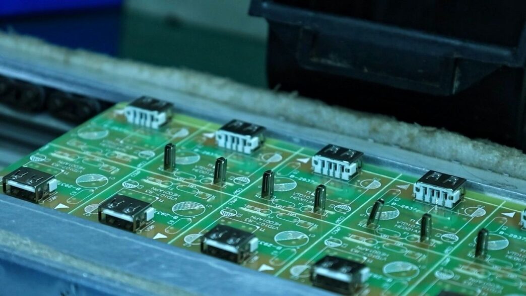
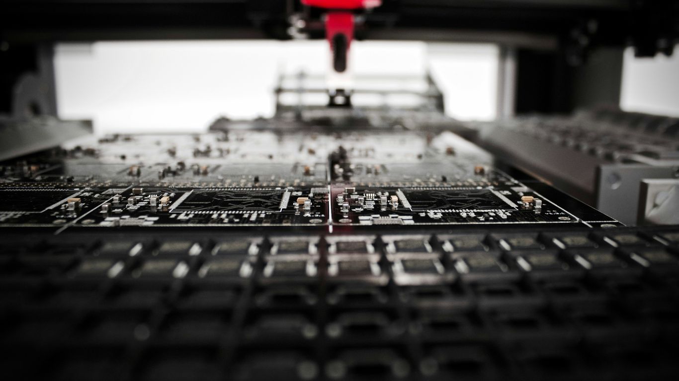
The Flip Chip IC Packaging Process
So, how do we actually get these tiny chips flipped and stuck onto a board? It’s not magic, though sometimes it feels like it. The flip chip packaging process is a multi-step journey that’s pretty different from the old-school wire bonding. It’s all about making direct connections, which is where the real benefits come in.
Wafer Bumping Techniques
Before you can even think about flipping a chip, you need to put little bumps on its connection points, called pads. This is the wafer bumping stage. Think of these bumps as tiny solder balls that will eventually connect to the substrate. There are a few ways to do this, and the method chosen often depends on what you’re trying to achieve:
- Solder Bumping: This is a common method where solder paste is applied to the pads, often using a stencil, and then heated to form the bumps. It’s pretty straightforward.
- Plated Bumping: Here, metal layers are electroplated onto the pads, and then a solder cap is added. This gives you more control over the bump’s size and shape.
- Stud Bumping: This involves placing small metal balls (studs) onto the pads, usually with an adhesive. It’s a bit less common for high-density applications but has its uses.
- Adhesive Bumping: Instead of solder, conductive adhesive is used to form the bumps. This can be good for certain types of substrates or when you need to avoid high reflow temperatures.
Die Alignment and Reflow Soldering
Once the bumps are ready on the wafer, it’s time to actually connect the chip to its new home – the substrate or PCB. This is where the "flip" part really happens.
- Alignment: The chip, with its bumps facing down, is carefully positioned over the corresponding pads on the substrate. This needs to be super precise, like lining up a needle with a tiny hole, but on a microscopic level.
- Reflow Soldering: After alignment, the whole assembly goes into a reflow oven. The heat melts the solder bumps, allowing them to flow and form a strong, direct electrical and mechanical connection with the substrate pads. This is what creates the solid bond.
Underfill Application for Reliability
Just sticking the chip down isn’t always enough, especially in demanding applications. The solder joints, while strong, can be a bit brittle. To make sure everything holds up over time, especially with temperature changes and vibrations, an underfill material is applied.
- What it is: It’s usually a type of epoxy or adhesive that flows into the gap between the chip and the substrate, right under the die.
- Why it’s important: This underfill material does a few key things. It mechanically reinforces the solder joints, spreading the stress more evenly. It also helps conduct heat away from the chip, which is a big deal for performance. Plus, it acts as a barrier against moisture and contaminants.
- The process: After the solder has cooled and the chip is attached, the underfill material is dispensed around the edges of the chip. Capillary action draws it underneath. Then, it’s cured, typically with heat, to harden it into place. This whole process really locks everything down and makes the flip chip assembly much more robust.
Applications and Industry Impact
Flip chip technology isn’t just some niche thing for super-specialized gear; it’s actually showing up everywhere, powering a lot of the tech we use daily. Think about your smartphone or the powerful computers crunching data for AI – flip chip is a big reason they work so well.
High-Performance Computing and Mobile Devices
When you need serious processing power, like in server chips or graphics cards (GPUs), flip chip is often the go-to. It handles the massive number of connections (I/O) these chips need and helps get heat away, which is super important when things are running at full tilt. This ability to pack in more connections and manage heat better is what lets us have faster computers and more capable mobile devices. Even your phone benefits, with flip chip packages helping to keep things small and speedy, especially with the demands of 5G. It’s all about getting signals where they need to go quickly and without a lot of interference.
Power Electronics and RF Applications
In power electronics, where you’re dealing with significant amounts of electricity, and in radio frequency (RF) applications for things like wireless communication, flip chip makes a difference. The shorter paths for electrical signals mean less signal loss and better performance, which is key for reliable communication and efficient power delivery. This technology is helping to make things like advanced driver assistance systems in cars and the infrastructure for faster wireless networks more robust.
Enabling System-in-Package (SiP) Solutions
Flip chip is also a big player in creating System-in-Package (SiP) solutions. Instead of just one chip, SiP combines multiple chips and components into a single package. Flip chip’s high I/O density and small footprint make it ideal for stacking these components efficiently. This allows for more complex functionalities to be packed into smaller spaces, which is a huge win for miniaturization in electronics. The market for flip chip technology is expected to keep growing, moving from an estimated USD 38.14 billion in 2026 to over USD 54 billion by 2031, showing just how important it’s becoming flip chip technology market.
Here’s a quick look at where you’ll find it:
- High-Performance Computing: Servers, workstations, AI accelerators.
- Mobile Devices: Smartphones, tablets, wearables, 5G infrastructure.
- Automotive: Advanced driver-assistance systems (ADAS), infotainment, engine control units.
- Consumer Electronics: High-end gaming consoles, smart TVs.
- Industrial: Automation, control systems, high-power modules.
Design and Manufacturing Considerations

Alright, so you’ve got this fancy flip chip idea, and you’re thinking about how to actually make it work. It’s not just about the chip itself, you know? You’ve got to think about the whole package, the board it’s going on, and how it’s all going to get put together. It’s a bit like building a house – you need a solid plan before you start hammering nails.
Design for Manufacturability and Assembly
This is where you make sure your design isn’t a nightmare to build. You don’t want to design something that looks great on paper but is impossible or super expensive to put together. Think about things like:
- Trace Width and Spacing: Make sure your circuit lines are wide enough and spaced far enough apart so they don’t accidentally touch or cause signal issues. Your substrate maker will have specific rules for this, and you gotta follow them.
- Pad Sizes: The little pads on your chip where the bumps connect need to match up with the pads on the substrate. If they’re off, you’re going to have a bad time during soldering.
- Alignment Markers: These are like little targets that the machines use to line up the chip perfectly. Without good ones, the whole process can go sideways.
- Underfill Details: You need to tell everyone what kind of underfill material to use and how to apply it. This stuff is important for making sure the bumps don’t break when the chip heats up and cools down.
Substrate Material Selection
The substrate, that’s the board the chip sits on, is a big deal. It’s not just a piece of plastic.
- CTE Mismatch: Different materials expand and contract at different rates when the temperature changes. If your chip and substrate expand too differently, it puts a lot of stress on those tiny solder bumps. You want materials that play nice together, like using substrates with a Coefficient of Thermal Expansion (CTE) that’s closer to the chip’s.
- Dielectric Constant (Dk) and Dissipation Factor (Df): For high-speed signals, these properties matter a lot. You need them to be consistent across the substrate to control how your signals travel and avoid unwanted reflections or signal loss.
- Thermal Properties: How well does the substrate conduct heat away from the chip? If your chip gets too hot, it won’t last long. Some materials are better at this than others.
Here’s a quick look at how some common substrate materials stack up:
| Material Type | CTE (ppm/°C) | Thermal Conductivity (W/mK) | Notes |
|---|---|---|---|
| FR-4 | 15-20 | 0.3-0.5 | Common, but high CTE mismatch |
| BT Resin | 10-15 | 0.5-1.0 | Better CTE, good for moderate temps |
| ABF (Ajinomoto Build-up Film) | 8-12 | 0.8-1.5 | Low CTE, good thermal, common for flip chip |
| Ceramic | 3-7 | 15-25 | Very low CTE, excellent thermal, but costly |
Reliability Testing and Troubleshooting
Even with the best design, things can go wrong. That’s why testing is super important. You need to make sure your flip chip assembly can handle the real world.
- Thermal Cycling: This is where you heat up and cool down the assembly over and over to see if the bumps or underfill crack.
- Vibration Testing: If the product is going to be shaken around, you need to test that too.
- Moisture Sensitivity: Some materials can absorb moisture, which can cause problems when heated. You’ll want to test for that.
If something does go wrong, you’ll need ways to figure out what happened. Tools like X-ray machines can look inside the package to see if there are any bad solder joints or voids in the underfill. Sometimes, you might find issues like:
- Open or Shorted Bumps: A bump might not connect properly, or two might touch when they shouldn’t.
- Underfill Voids: Gaps in the underfill can lead to stress points.
- Die or PCB Warping: The chip or board might bend, causing problems.
It’s all about planning ahead and testing thoroughly to make sure your flip chip design actually works and keeps working.
Future Trends in Flip Chip IC Technology
So, what’s next for flip chip IC technology? It’s not just about making things smaller, though that’s definitely part of it. The industry is pushing boundaries in a few key areas, and it’s pretty exciting to see where it’s all heading.
Advanced Interconnect Materials
We’re seeing a big push towards new materials for those little bumps that connect the chip to the substrate. Think beyond just solder. Researchers are looking at things like copper pillars and even novel conductive adhesives. The goal is to get even finer pitches, which means more connections in the same space, and better reliability, especially when dealing with lead-free requirements. These new materials are key to handling the increasing demands of high-speed data and complex processing. It’s all about making those connections more robust and efficient.
Heterogeneous Integration and Chiplets
This is a huge one. Instead of trying to cram everything onto one giant chip, the trend is towards "chiplets." These are smaller, specialized chips that are then put together on a single package using flip chip technology. It’s like building with LEGOs, but for electronics. This approach allows for mixing and matching different types of silicon (like CPUs, GPUs, and AI accelerators) from different foundries, all optimized for their specific tasks. It’s a really smart way to build complex systems without the massive cost and yield issues of monolithic designs. We’re already seeing this in high-end processors, and it’s only going to become more common.
Cost Reduction and Miniaturization Innovations
Let’s be real, cost is always a factor. As flip chip technology matures, there’s a constant drive to make the manufacturing processes more efficient and less expensive. This involves everything from optimizing wafer bumping techniques to streamlining the assembly line. At the same time, the demand for smaller, more powerful devices in everything from smartphones to wearables means miniaturization is still a major focus. Innovations in underfill materials and advanced substrate designs are helping to pack more functionality into smaller footprints while maintaining reliability. It’s a balancing act, but one that’s essential for keeping electronics accessible and pushing the limits of what’s possible.
Wrapping It Up
So, we’ve gone over what flip chip technology is all about. It’s pretty neat how it lets us connect chips directly, making things smaller and faster. This method is really changing the game for all sorts of electronics, from your phone to big computers. As we keep needing more power and smaller gadgets, flip chip is going to be a big part of that. It’s not just a fancy way to build chips; it’s what’s going to let us build the next wave of cool tech. Anyone working with electronics these days really needs to get a handle on this stuff if they want to stay ahead of the curve.
Frequently Asked Questions
What exactly is flip chip technology?
Imagine a tiny computer chip, like the brain of your phone. Instead of connecting it with thin wires, flip chip technology flips the chip upside down and sticks it directly onto a board using tiny solder bumps. This makes the connections much shorter and faster.
How is flip chip different from old-fashioned wire bonding?
Think of wire bonding like using tiny threads to connect the chip to the board. Flip chip is more like using little metal pillars to connect directly. This makes flip chip way better for speed and handling heat because the connections are shorter and thicker.
Why is flip chip so good for making electronics smaller and faster?
Because the connections are so short, signals can travel faster, making the chip work quicker. Also, since the chip is flipped and connected directly, you can pack more connection points (called I/Os) into the same space, allowing for more complex and smaller devices.
Does flip chip help keep chips cool?
Yes! Since the chip is attached directly to the board, heat can escape more easily. This is like having a better way for the chip to ‘sweat’ and cool down, which is super important for powerful chips that get hot.
What is ‘underfill’ and why is it used with flip chips?
Underfill is like a special glue put around the solder bumps after the chip is attached. It helps spread out any stress from heat or bumps, making the connection stronger and preventing it from breaking over time, especially in devices that get moved around a lot or experience temperature changes.
Can flip chip technology be used in all electronics?
Flip chip is mostly used in electronics that need to be super fast and powerful, like in high-end computers, smartphones, and gaming consoles. For simpler or cheaper devices, other methods might still be used, but flip chip is becoming more common as we need more performance.