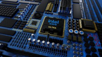
When you hear tech folks talking about CPUs and their “nanometer” sizes, it can sound like a different language. What does 5nm even mean? It’s not about tiny ants, but it is a big deal for how your gadgets work. The size, measured in nanometers, is a key part of making chips, and it really changes how well your computer’s brain performs, how much power it uses, and how hot it gets. Today, we’re going to look into this world of chip making, figure out what these nanometer numbers mean, why smaller is usually better, and how this small-scale advantage is shaping tomorrow’s tech. Ready to get a little nerdy? Let’s go!
Key Takeaways
- The ‘nanometer’ number in chip manufacturing refers to the size of the smallest parts, like transistor gates. A 5nm process means these parts are incredibly small, about 5 billionths of a meter.
- Smaller transistors mean more can fit on a chip, leading to more computing power and faster performance.
- Smaller transistors also use less power, which means longer battery life and less heat in your devices.
- Making these tiny transistors is super expensive and runs into physical limits, so chipmakers are always looking for new ways to build them.
- The trend towards smaller sizes impacts more than just CPUs, affecting graphics chips, smartphone components, and AI hardware too.
Understanding the 5 Nanometer Transistor
What Does Nanometer Size Mean in Chip Manufacturing?
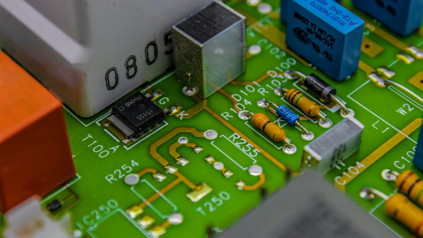
When you hear about chips being made with a "5 nanometer" process, it sounds super technical, right? But what does that number actually mean? It’s not about the size of the whole chip, not even close. Instead, that ‘nm’ number refers to the size of the smallest parts etched onto the silicon, specifically the length of the transistor’s gate. Think of it like the resolution on a printer – a smaller nanometer number means the manufacturer can draw much finer details. So, a 5nm process means the tiniest features are about 5 billionths of a meter. This is a huge leap from older chips, where features were much larger, limiting how many transistors could fit. The ability to shrink these components is what allows us to pack more processing power into smaller devices.
A Brief History of Process Node Evolution
Chip manufacturing has come a long way. Back in the early 2000s, we were talking about 130nm and 90nm processes. Then, things started shrinking rapidly. By the mid-2000s, we saw 65nm and 45nm nodes become common. The 2010s brought us down to 32nm, 22nm, and eventually 14nm. Each step down in nanometers meant more transistors could be squeezed onto a single chip, leading to faster and more efficient processors. This constant drive to shrink has been a hallmark of the semiconductor industry for decades, pushing the boundaries of what’s possible in electronics. It’s a story of continuous innovation, with each generation of chips building on the successes of the last.
| Process Node (nm) | Approximate Timeframe |
|---|---|
| 130 – 90 | Early 2000s |
| 65 – 45 | Mid-2000s |
| 32 – 14 | 2010s |
| 5 | Present |
The Significance of Smaller Transistors
So, why all the fuss about making transistors smaller? It boils down to a few key benefits. First, you can fit way more transistors onto the same piece of silicon. This increased transistor count means more complex calculations can happen simultaneously, leading to better performance. Second, smaller transistors generally use less power. Imagine tiny light switches versus big, clunky ones; the smaller ones require less energy to flip. This is a big deal for battery life in phones and laptops. Finally, all these smaller, more efficient transistors working together can make your devices run faster. It’s a trifecta of improvements: more power, less energy used, and quicker operations. This is why the race to smaller nanometer processes is so important for the future of computing and all sorts of electronic devices.
The Advantages of a 5 Nanometer Process
So, why all the fuss about 5 nanometer (nm) chips? It boils down to some pretty sweet benefits that make our gadgets faster, last longer on a charge, and generally just work better. It’s not just about bragging rights in the tech world; these improvements have real-world impacts.
Increased Transistor Density
Think of transistors as the tiny on/off switches that make your computer’s brain, the CPU, do its thing. When you shrink the manufacturing process down to 5nm, you can cram way more of these switches onto the same piece of silicon. It’s like going from a sprawling single-story house to a multi-story apartment building on the same plot of land. More transistors mean more processing power. This allows your devices to handle more complex calculations and run demanding applications without breaking a sweat. It’s the primary reason why newer chips can do so much more than their older, larger counterparts.
Reduced Power Consumption
Smaller transistors don’t need as much juice to operate. This is a huge win for battery-powered devices like smartphones and laptops. Less power used means your battery lasts longer, so you can stream more videos or get more work done between charges. Plus, less power consumption usually means less heat generated. Nobody likes a laptop that feels like a hot plate after an hour, right? This also means devices can be designed to be thinner and lighter because they don’t need massive cooling systems. It’s a win-win for both the user and the device’s design.
Enhanced Performance Capabilities
When you pack more transistors and reduce the distance they need to communicate, things just move faster. The 5nm process allows for quicker data processing and signal transmission. This translates directly into snappier performance for everything you do on your device. Apps load faster, games run smoother, and multitasking becomes a breeze. It’s the combination of more transistors and more efficient operation that really makes a difference. For example, graphics processing units (GPUs) benefit immensely, allowing for more detailed visuals and faster rendering in games and creative applications. The advancements in TSMC’s 5nm process show just how much yield can be achieved, paving the way for widespread adoption and performance gains across the industry.
Beyond CPUs: Impact Across Technologies
While we often talk about CPUs when discussing these tiny transistors, their influence stretches way beyond just the main processor in your computer. Think about all the other smart devices and components that make our tech work. The push for smaller, more efficient transistors is a big deal for them too.
Graphics Processing Units (GPUs)
Graphics cards, or GPUs, are basically specialized processors designed for handling all the visual stuff – think video games, complex simulations, and video editing. Just like CPUs, GPUs get a serious boost from smaller transistor sizes. More transistors packed into the same space means they can crunch more graphics data, leading to smoother frame rates and more detailed visuals. Plus, they can do all this while using less power, which is great for keeping your gaming rig from sounding like a jet engine.
System-on-Chip (SoC) Designs
These are the brains behind your smartphone, tablet, and many other portable gadgets. A System-on-Chip, or SoC, is like a whole computer system crammed onto a single piece of silicon. It includes the CPU, GPU, memory controllers, Wi-Fi radios, and all sorts of other bits and pieces. Using 5nm (or even smaller) processes allows manufacturers to pack all these functions into a tiny space, keep power consumption low for better battery life, and still deliver impressive performance. It’s how we get super-powerful phones that fit in our pockets.
Specialized AI Accelerators
Artificial intelligence is everywhere now, from voice assistants to complex data analysis. Running AI models, especially deep learning algorithms, requires a lot of computational power. Specialized chips, often called AI accelerators or Neural Processing Units (NPUs), are designed specifically for these tasks. The smaller transistor sizes found in 5nm technology are a perfect fit for these chips. They allow for a massive number of calculations to be performed very quickly and with minimal power draw, making on-device AI processing a reality without draining your battery in minutes.
Challenges in Manufacturing Tiny Transistors
Making transistors smaller and smaller, like down to the 5-nanometer mark and beyond, sounds like a win-win, right? More power, less energy used. But getting there is a real headache for chip makers. It’s not just about having a really good magnifying glass; it’s a whole bunch of tough problems.
Escalating Production Costs
First off, it costs a fortune. The machines needed to etch these tiny patterns, like the fancy EUV lithography tools, can run into hundreds of millions of dollars each. Then there’s the research and development to even figure out how to make these smaller nodes work, which can cost billions. This means only a few big companies, like TSMC, Samsung, and Intel, can even afford to play in this super-advanced manufacturing space. It’s like trying to build a Formula 1 car with a regular garage toolkit – just not feasible for most.
Navigating Physical and Quantum Limits
As transistors shrink down to just a few atoms across, things get weird. We’re talking about quantum mechanics here. Electrons, those tiny little things that carry the electrical signals, can start to ‘tunnel’ through barriers they’re not supposed to cross. Imagine a ball rolling towards a small hill; normally, if it doesn’t have enough speed, it stops. But in the quantum world, that ball might just appear on the other side of the hill. In chips, this ‘tunneling’ causes unwanted electrical leakage and makes the chip unstable. Plus, controlling things at the atomic level means even tiny imperfections or variations can ruin a chip, leading to lower production yields – meaning fewer working chips from each silicon wafer.
Managing Thermal and Power Density
Even though individual transistors use less power when they’re tiny, packing billions of them incredibly close together creates a new problem: heat. The overall heat generated in a small area, known as thermal density, can become a major issue. If not managed properly, these super-fast chips can overheat, leading to performance problems or even damage. This means engineers have to get really creative with cooling solutions and how the chip is designed to spread out that heat, which adds another layer of complexity to the manufacturing process.
Innovations Driving Nanometer Advancements

Advanced Transistor Architectures
Making transistors smaller isn’t just about shrinking existing designs. As we get down to the 5nm scale and beyond, traditional transistor designs start to run into physical limits. Electrons can get a bit too eager and "tunnel" through barriers they’re supposed to stay behind, causing unwanted leakage and errors. To get around this, chipmakers are using smarter designs. Think of FinFETs, which have a "fin" that sticks up, giving the gate more control over the channel. Even newer are Gate-All-Around (GAA) FETs, where the gate wraps all the way around the channel, offering even better control. It’s like upgrading from a simple light switch to a dimmer with a much finer adjustment.
Novel Materials in Fabrication
Beyond just the shape of the transistor, the materials used are changing too. Old-school transistors used simple silicon dioxide for insulation. But at these tiny scales, that just doesn’t cut it anymore. Newer chips use "high-k dielectrics" and "metal gates." These materials help reduce leakage current and allow transistors to switch on and off more reliably and quickly. It’s a bit like using a better quality wire and insulation for your electrical system – it just works better and more efficiently.
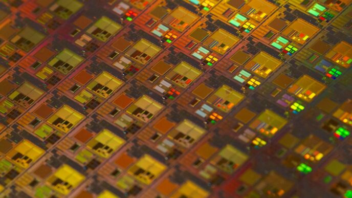
Complex Multi-Layer Manufacturing
Building a modern chip is incredibly complex. It’s not just one layer; it’s dozens of them, stacked precisely on top of each other. Each layer involves etching, doping, and depositing materials with nanometer-level accuracy. Imagine building a skyscraper, but each floor is thinner than a human hair, and you have to get every single connection perfect. This multi-layer approach allows for intricate wiring and component placement, packing more functionality into a tiny space. It’s a bit like assembling a super-detailed miniature model, where every piece has to fit just right for the whole thing to work.
The Future of Semiconductor Manufacturing
Exploring Sub-Nanometer Processes
So, what’s next after we’ve squeezed transistors down to 5 nanometers and even smaller? It’s not just about making things tinier for the sake of it. The industry is looking at processes below 3nm and even 2nm. This isn’t just a simple scaling down; it involves rethinking how transistors are built. We’re talking about new materials that can handle these incredibly small sizes without losing their cool, and different ways to arrange transistors, like Gate-All-Around (GAA) designs, which offer better control than older FinFETs. It’s a constant push to get more power and efficiency out of silicon, even as we bump up against what seems physically possible.
The Role of Chiplets
Instead of trying to cram everything onto one giant, super-complex chip, the future is also about "chiplets." Think of it like building with LEGOs. You have smaller, specialized chips (the chiplets) that are designed to work together. One chiplet might handle the main processing, another the graphics, and yet another the AI tasks. These chiplets are then packaged together. This approach makes manufacturing easier and more cost-effective because you can test each chiplet individually. Plus, if one part needs an upgrade, you can swap out just that chiplet instead of redesigning the whole thing. It’s a more modular way to build powerful computing systems.
Rethinking Measurement Metrics
For a long time, the "nanometer" number – like 5nm or 3nm – was the main way we talked about how advanced a chip process was. But honestly, that number has become a bit confusing and doesn’t always tell the whole story. Some experts even think it’s become meaningless. They’re looking for new ways to measure progress that are clearer and more useful. This could involve metrics that look at how well different parts of a chip work together, or how much computing power you get for the energy used, rather than just a size label. The goal is to have a way to track advancements that truly reflects the real-world performance and capabilities of these tiny technological marvels.
So, What’s the Big Deal with 5 Nanometers?
Alright, so we’ve talked a lot about these tiny 5-nanometer transistors. Basically, they’re the reason your phone doesn’t overheat and your laptop feels super snappy. Making things this small is a huge engineering feat, and it’s not easy or cheap. Chip companies are always pushing to make them even smaller, but there are real limits, like weird quantum stuff happening. Even though smaller numbers usually mean better performance and less power used, it’s not the only thing to look at when you’re picking out a new gadget. Just remember, the next time you’re using your tech, there are billions of these little guys working hard inside. It’s pretty wild to think about, and who knows what they’ll come up with next!
Frequently Asked Questions
What does the ‘5 nanometer’ in 5nm transistor actually mean?
The ‘5 nanometer’ (nm) number doesn’t refer to the whole chip. Instead, it tells us the size of the smallest parts on the chip, like the tiny switches called transistors. A 5nm process means these parts are incredibly small, about 5 billionths of a meter. Think of it like the resolution on a screen – a smaller number means more detail and smaller components.
Why are smaller transistors better?
Smaller transistors mean we can pack way more of them onto a single chip. More transistors mean a chip can do more things, work faster, and handle complex tasks more easily. Plus, smaller transistors use less energy, which helps your devices last longer on a battery and keeps them from getting too hot.
Does 5nm technology only apply to computer processors (CPUs)?
No, it’s not just for CPUs! This advanced technology is also used in graphics cards (GPUs) that make games and videos look amazing, and in System-on-Chip (SoC) designs found in smartphones and tablets. It’s even used in special chips that help artificial intelligence (AI) learn and work faster.
Are there any problems with making transistors so small?
Yes, there are big challenges! Making these tiny parts costs a lot of money, with special machines costing hundreds of millions of dollars. Also, when things get this small, strange things happen due to quantum physics, like electrons jumping where they shouldn’t. It’s also tricky to manage the heat these tiny, powerful components can create.
What comes after 5nm technology?
The tech world is always looking ahead! Engineers are already working on even smaller sizes, like 3nm and 2nm processes. They are also exploring new materials and ways to build chips, like using ‘chiplets’ – small, specialized chip pieces put together – instead of one giant chip.
Is it possible to keep making transistors smaller forever?
It’s unlikely we can keep shrinking transistors made of traditional materials like silicon indefinitely. We’re getting close to the size of atoms, where quantum effects become very difficult to control. However, engineers are finding clever ways to improve chips using new designs, materials, and ways of putting chips together, so progress will likely continue in different forms.