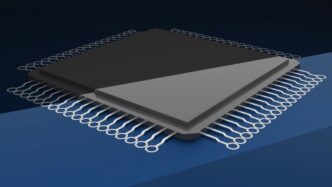

So, what exactly is a chiplet? Think of it like building with LEGOs, but for computer chips. Instead of one giant, complicated piece, we’re now assembling systems from smaller, specialized blocks. This shift from the old way of doing things, where everything had to be on a single chip, is a pretty big deal. It’s changing how we make electronics, making them faster, more efficient, and easier to upgrade. Let’s break down what this chiplet revolution is all about.
Key Takeaways
- Chiplets are small, independent pieces of a chip, each designed for a specific job, that are put together using advanced packaging.
- This modular approach moves away from older, single-piece chip designs, offering more flexibility and better performance.
- Chiplets allow for mixing and matching different technologies and manufacturing processes, speeding up innovation and improving how many good chips can be made from a wafer.
- Putting chiplets together brings challenges like complex connections, testing, and managing heat, but the industry is working on solutions and standards.
- The chiplet market is growing fast, opening up new opportunities for companies and driving the development of more powerful and specialized electronic devices.
Understanding What Is A Chiplet
So, what exactly is a chiplet? Think of it like building with LEGOs, but for computer chips. Instead of making one giant, complicated piece for everything, we break it down into smaller, specialized blocks. These smaller blocks are what we call chiplets.
Defining Chiplets As Modular Dies
Basically, a chiplet is a small, self-contained piece of silicon that does a specific job. It’s like a mini-chip designed to work with other mini-chips. These aren’t just random bits; they’re pre-designed and tested components. You can think of them as modular dies – individual units that can be combined to form a larger system. This is a big change from how things used to be done.
The Shift From Monolithic Designs
For a long time, the standard way to make chips was the monolithic approach. This meant cramming all the necessary functions – like the processor, graphics, and memory controllers – onto a single, large piece of silicon. It worked, but as chips got more complex, this method started hitting some walls. Making these huge chips perfectly is tough, and if even a small part has a defect, the whole thing can be useless. Plus, designing them became incredibly expensive and time-consuming.
Chiplets offer a different path. Instead of one big chip, you have several smaller ones, each handling a specific task. For example, you might have one chiplet for the CPU cores, another for the graphics, and maybe a third for input/output. These chiplets are then put together using advanced packaging techniques, almost like snapping those LEGOs together.
Core Functionalities Of Chiplets
Chiplets are designed to be specialized. You’ll find chiplets for:
- Processing: These are the brains, handling calculations and running software. Think CPU cores or AI accelerators.
- Memory: Some chiplets might be dedicated to managing or storing data.
- Input/Output (I/O): These handle communication with the outside world, like connecting to networks or peripherals.
- Specialized Accelerators: Chiplets can be built for very specific tasks, like video encoding or advanced graphics processing, using the best manufacturing process for that particular job.
This modularity means designers can pick and choose the best chiplets for their needs, rather than being stuck with whatever fits on a single monolithic design. It’s a more flexible and efficient way to build powerful computing systems.
Revolutionary Advantages Of Chiplet Technology
So, why all the fuss about chiplets? It turns out breaking down big chips into smaller, specialized pieces brings some pretty sweet benefits. It’s not just a minor tweak; it’s a whole new way of thinking about how we build the brains of our devices.
Enhanced Performance Through Specialization
Think of it like building a specialized team instead of one person trying to do everything. With chiplets, you can pick the absolute best chiplet for each specific job. Need a super-fast graphics processor? Grab the best GPU chiplet. Need a powerful AI accelerator? There’s a chiplet for that too. This means each part of the system is designed to do its one thing exceptionally well, leading to overall better performance than a single, do-it-all chip that has to compromise on some functions.
Accelerated Innovation And Time-To-Market
This modular approach really speeds things up. Instead of designing a massive, complex chip from scratch every single time, companies can use pre-made, tested chiplets. It’s like using LEGO bricks instead of carving a sculpture from a single block of stone. This means new products can get out the door much faster, which is a big deal in the fast-paced tech world. Plus, if a company needs a custom solution, they can mix and match existing chiplets to create something unique without starting from zero.
Improved Manufacturing Yields
Making really big, complex chips is tough. The bigger the chip, the higher the chance of a tiny defect ruining the whole thing. Smaller chiplets are just easier to manufacture successfully. If one small chiplet has a problem, you only lose that one small piece, not an entire giant chip. This means fewer wasted wafers and a better overall production rate, which can help keep costs down.
Greater Design Flexibility And Customization
Chiplets give designers a lot more freedom. They aren’t locked into one company’s monolithic design. They can pick and choose chiplets from different vendors, combining the best available technologies. This allows for highly customized solutions tailored to very specific needs, whether it’s for a high-end server, a specialized AI device, or even a niche consumer gadget. It opens up possibilities for creating exactly what’s needed, without being limited by traditional design constraints.
Key Advanced Packaging Techniques For Chiplets
So, we’ve got these individual chiplets, right? They’re like LEGO bricks for processors. But how do we actually stick them all together to make something useful? That’s where advanced packaging comes in. It’s not just about putting chips in a box anymore; it’s a whole sophisticated process.
2.5D And 3D Integration Methods
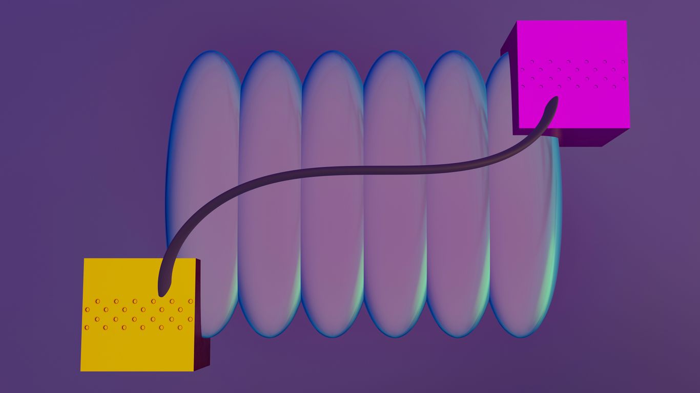
Think of 2.5D and 3D integration as stacking or arranging chiplets in clever ways. With 2.5D, chiplets are placed side-by-side on a special silicon or organic layer called an interposer. This interposer has tiny wires that connect the chiplets. It’s like a mini-highway system just for the chiplets. 3D integration takes it a step further by stacking chiplets on top of each other. This requires really tiny vertical connections, often called through-silicon vias (TSVs), to link the layers. This stacking gets the chiplets super close, cutting down the distance signals have to travel, which means faster speeds and less power used. It’s a big deal for packing more power into a smaller space.
The Role Of Hybrid Bonding
Now, hybrid bonding is a pretty neat trick. Instead of using traditional wire bonds or bumps to connect chiplets, hybrid bonding directly joins the metal pads of two chips together. It’s like a direct handshake between the chiplets. This allows for incredibly fine connections, way more than you can get with older methods. The catch? Both chiplets need to be super flat and perfectly aligned. It’s a bit like trying to perfectly stack two pieces of glass. But when it works, the density of connections is amazing, leading to even better performance.
Fan-Out Wafer-Level Packaging Innovations
Fan-out wafer-level packaging, or FOWLP, is another way to get those high-density connections. Instead of building the connections on a separate interposer, FOWLP builds them directly around the chiplets on a wafer. It essentially creates a redistribution layer (RDL) that fans out from the chiplet, allowing more connections to be made. This can be more cost-effective than some other methods and is great for fitting more connections into a package.
Heterogeneous Integration Approaches
This is where things get really interesting. Heterogeneous integration is all about mixing and matching different types of chiplets, even if they were made using completely different manufacturing processes. You could have a high-performance CPU chiplet made on one process node, a memory chiplet from another, and maybe a special AI accelerator chiplet, all put together in the same package. This modularity lets designers pick the best chiplet for each job, rather than trying to cram everything onto one giant, monolithic chip. It’s the ultimate customization for building complex systems.
Navigating Chiplet Integration Challenges
So, chiplets sound pretty great, right? Smaller pieces, specialized jobs, easier manufacturing. But putting them all together isn’t exactly a walk in the park. There are definitely some hurdles to clear before this whole chiplet thing becomes as common as, well, regular chips.
Addressing Interconnect Complexity
Think of chiplets as tiny Lego bricks. You need a way to connect them so they can talk to each other. This connection, or interconnect, needs to be super fast and handle a lot of data. Designing these connections is tricky. You’ve got to figure out how to pack a lot of tiny wires very close together without them interfering with each other. This often involves special layers in the packaging, like interposers or redistribution layers (RDLs), which add their own manufacturing steps and costs. Getting these high-speed, high-density links to work reliably is a big deal.
Ensuring Rigorous Testing and Validation
When you have one big chip, you test the whole thing. With chiplets, you’ve got multiple smaller pieces. You need to test each chiplet individually to make sure it’s "known good" before you even try to put it into the final package. Then, you have to test the whole assembled chiplet system to make sure everything works together as planned. This "known-good-die" (KGD) approach is vital. It’s like making sure every single Lego brick is perfect before you start building your castle, and then checking the whole castle when it’s done.
Effective Thermal Management Strategies
All these little chiplets packed closely together generate heat. A lot of heat, sometimes. If you can’t get that heat away efficiently, performance suffers, and things can even get damaged. So, designers have to get creative with cooling. This might mean using special materials to spread the heat out, adding heat sinks, or designing the package itself to help with airflow. It’s a constant balancing act between packing more power and keeping things from overheating.
The Drive For Industry Standardization
Right now, there isn’t one single way everyone agrees on to connect chiplets. Different companies might use different "languages" or connection methods. This makes it hard for chiplets from one company to work with chiplets from another. Imagine trying to connect Lego bricks from different brands – some might not fit! That’s why there’s a big push for common standards. This would allow for a more open market where you can mix and match chiplets from various vendors, much like how USB ports work for different devices today. It’s a work in progress, but getting these standards in place is key for chiplets to really take off.
The Evolving Chiplet Marketplace
Impact On Fabless Companies
So, what does all this chiplet stuff mean for companies that design chips but don’t actually make them (the fabless ones)? Well, it’s pretty interesting. Imagine a world where there are lots of ready-made, tested chiplets available from different companies. A smaller, newer fabless company could grab a few of these pre-built pieces, maybe add just one or two of their own custom bits, and boom – they’ve got a new product. This could make it way easier for new players to get into the game. It means they don’t have to design everything from scratch, which is super expensive and time-consuming. They can focus their efforts on what makes their product unique, letting others handle the more common chip functions.
Multi-Vendor Supply Chain Opportunities
This whole chiplet idea is really opening doors for a bunch of different companies to work together. Instead of one big company making a whole chip, you can have specialists. One company might make the best CPU chiplet, another the best graphics chiplet, and someone else the best memory interface chiplet. Then, a third company, or even the chip designer themselves, can put these pieces together using advanced packaging. This creates a whole ecosystem where different vendors can supply parts, leading to more competition and potentially better prices and performance for everyone. It’s like building with LEGOs, but for super-advanced electronics.
The Role Of Common Frameworks
For this multi-vendor marketplace to really take off, though, things need to be standardized. Companies need to agree on how these chiplets talk to each other – the interfaces, the communication protocols, all that technical stuff. Without common frameworks, it’s like trying to connect LEGO bricks from different brands that don’t quite fit. Industry groups are working hard on this, trying to create shared standards so that a chiplet made by Company A will work perfectly with one made by Company B. This collaboration is key to making chiplet designs more accessible and predictable for everyone involved.
Future Trajectories Of Chiplet Design
Continued Development Of Standardized Interfaces
So, where are chiplets headed next? One big area is making sure all these little pieces can talk to each other easily. Right now, there’s a lot of work going into creating common ways for chiplets to connect. Think of it like USB for computer parts – you can plug in almost anything, and it just works. The goal is to get to a point where chiplets from different companies can be mixed and matched without a huge headache. This means defining standard communication protocols and physical interfaces. It’s a slow process, involving lots of companies collaborating, but it’s super important for making chiplets truly flexible and widely adopted. Without these standards, we’re stuck with a bunch of proprietary systems that don’t play well together.
Increased Heterogeneous Integration
We’re going to see more and more different types of chiplets being put together. It’s not just about combining multiple CPU cores anymore. Imagine a package with a main processor, a specialized AI accelerator, a memory chip, and maybe even some optical components, all working as one. This is called heterogeneous integration, and chiplets are the perfect way to achieve it. Each chiplet can be made using the best manufacturing process for its specific job. For example, a high-performance logic chiplet might use the latest, most advanced manufacturing node, while a simpler I/O chiplet could use an older, more cost-effective one. This allows designers to build incredibly powerful and efficient systems tailored to very specific tasks, something that’s really hard to do with a single, giant monolithic chip.
Co-Design And Co-Optimization Trends
Looking further ahead, we’ll likely see more ‘co-design’ and ‘co-optimization’. This means that instead of designing chiplets and the package they go into separately, designers will consider them together from the very beginning. They’ll think about how the chiplets connect, how heat is managed, and how power is distributed across the entire package as a single system. This holistic approach can lead to even better performance and efficiency. It’s like building a custom car where every part, from the engine to the suspension, is designed to work perfectly with all the others, rather than just bolting on off-the-shelf components. This level of integration will push the boundaries of what’s possible in chip technology.
Environmental And Societal Implications
So, we’ve talked a lot about how chiplets are changing the tech game, making things faster and more flexible. But what about the bigger picture? Like, how does this whole chiplet thing affect our planet and, you know, us?
It turns out, there are some pretty interesting angles here. For starters, think about waste. Building those giant, single chips – monolithic designs – can be a real gamble. If there’s a tiny flaw somewhere in that massive piece of silicon, the whole thing might be useless. That’s a lot of wasted material and energy. Chiplets, being smaller and modular, can actually help with this. If one small chiplet has an issue, you might only need to replace that one piece, not the entire system-on-a-chip. This could mean less material used overall and less electronic waste piling up.
Sustainability Through Reduced Material Usage
This modular approach is a big deal for sustainability. Instead of fabricating a huge, complex chip where a single defect can ruin the entire wafer, chiplets allow for smaller, more manageable pieces. This means:
- Higher Manufacturing Yields: Smaller chiplets are generally easier to produce without defects. This leads to fewer wasted wafers and less raw material consumption.
- Reduced Material Waste: When a chiplet fails, it’s often easier and more efficient to replace just that component rather than discarding an entire large, monolithic chip.
- Optimized Material Use: Designers can pick and choose the best chiplets for specific tasks, potentially using less exotic or less material-intensive processes for certain functions.
Enabling Energy-Efficient Functionalities
Beyond just reducing waste, chiplets can also play a role in making our devices more energy-efficient. Think about it: instead of cramming every single function onto one giant chip that might have to power up even when parts aren’t being used, you can use specialized chiplets. You might have a super-efficient chiplet just for handling basic input/output, and another powerful one for heavy-duty processing, only activating when needed. This kind of targeted power management can lead to significant energy savings, especially in devices that are always on or performing complex tasks like AI processing. This focus on energy efficiency is becoming increasingly important as the demand for computing power, particularly for AI, continues to skyrocket. Making these advanced computations less power-hungry is key to a more sustainable technological future. It’s not just about making things smaller; it’s about making them smarter and more mindful of their energy footprint, which is something we can all get behind. For more on how technology is trying to be greener, you can check out predictive maintenance tools.
The Chiplet Revolution is Just Getting Started
So, that’s the lowdown on chiplets. It’s not just some fancy tech buzzword; it’s a real shift in how we build the brains of our gadgets. Instead of one giant, complicated chip, we’re now piecing things together with smaller, specialized bits. This whole approach means we can make things faster, more efficient, and even customize them better than before. While there are still some kinks to work out, like making sure all these little pieces talk to each other properly, the future looks bright. Chiplets are set to power the next wave of innovation, making our devices smarter and more capable than we can even imagine right now.
Frequently Asked Questions
What exactly are chiplets?
Think of chiplets as small, specialized building blocks for computer chips. Instead of making one giant, complicated chip, companies break it down into smaller, individual pieces, like LEGO bricks. Each chiplet does a specific job, like handling graphics or processing data. These smaller pieces are then put together using special techniques to create a powerful final chip.
Why are chiplets better than the old way of making chips?
In the past, all the parts of a chip were crammed onto one big piece of silicon, called a monolithic design. This got really expensive and hard to make perfectly as chips became more complex. Chiplets are like a smart upgrade. They let companies use the best manufacturing methods for each small piece, mix and match different types of chiplets, and fix problems more easily. This makes designing new chips faster, cheaper, and allows for more powerful computers.
What are the main benefits of using chiplets?
Chiplets offer a bunch of cool advantages! They help make chips perform better because each part is super specialized. They speed up how quickly new technology gets to us because designers can reuse existing chiplets. Making smaller chiplets means fewer mistakes during manufacturing, leading to better quality. Plus, designers have way more freedom to create custom solutions by picking and choosing the right chiplets.
Are there any difficulties with using chiplets?
Putting chiplets together isn’t always simple. Connecting all these tiny pieces requires very advanced and precise methods, which can be tricky. Making sure all the chiplets work perfectly together and testing the final product is also a challenge. Plus, because they’re packed so closely, managing the heat they produce is super important. We also need everyone to agree on common ways to design and connect them so different companies’ chiplets can work together.
How do chiplets help the environment?
Chiplets can be kinder to the planet. By breaking down big chips into smaller ones, we might use less raw material overall. Also, we can use very energy-efficient chiplets for specific tasks, making the whole device use less power. This means less waste and more sustainable technology in the long run.
What’s next for chiplets?
The future looks bright for chiplets! We’ll see even more standards so different chiplets can easily work together. Expect to see more complex systems built by combining many different kinds of chiplets, like processors, memory, and special AI chips. Designers will get even smarter about how they create and optimize these chiplet combinations to push the limits of what computers can do.