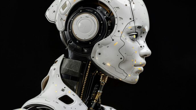
Chiplet technology is shaking up how chips are made and used. Instead of building one big chip from start to finish, companies can now piece together smaller, specialized chiplets to make a final product. This modular approach is gaining steam in 2025 because it helps tackle problems like rising costs, design complexity, and supply chain headaches. Whether you’re into AI, gaming, or just curious about how your phone gets faster every year, chiplets are a big reason why things are changing so quickly in the world of semiconductors. Let’s break down what chiplet technology is, why it’s important, and where it’s heading next.
Key Takeaways
- Chiplet technology means building chips from smaller, reusable parts instead of one big piece.
- This approach makes it easier and cheaper to upgrade or customize chips for different uses.
- Chiplets help companies avoid supply chain problems by letting them buy parts from different suppliers.
- New packaging and connection standards are making chiplets work faster and more reliably.
- Chiplets are already powering advances in AI, 5G, and consumer gadgets, but challenges like heat and design complexity remain.
Understanding Chiplet Architecture and Modular Design
Defining Chiplets and Their Role in Semiconductors
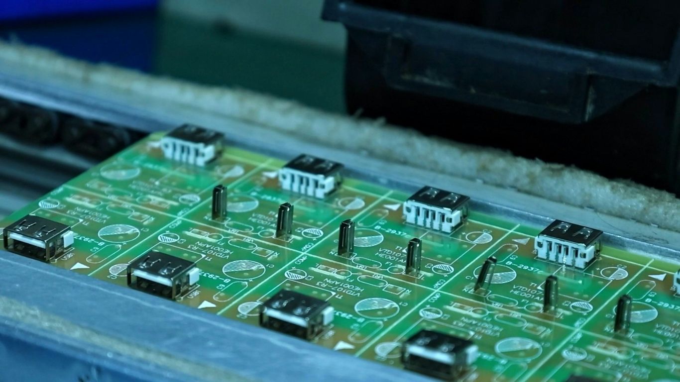
Chiplet technology is pretty much like breaking a big, complicated system-on-chip into several smaller pieces, each with its own job. Instead of cramming all your processing, memory, and connectivity functions onto one giant slab of silicon, engineers create these tiny chiplets; each one does something specific. You can think of chiplets as puzzle pieces that fit together to make one complete chip, only you can change out individual pieces if you want something different. These parts get connected using advanced packaging, and they’re all designed to work smoothly together. That’s especially handy for companies building high-performance hardware for AI, servers, or data centers. Chiplets make it possible to update one function (like adding faster memory or better I/O) without redesigning the whole thing.
Comparing Monolithic vs. Chiplet System-on-Chip Approaches
In the past, almost all chips were monolithic. You’d take one big piece of silicon and try to cram all the features on it—CPU, GPU, memory, you name it. If there was a design flaw or manufacturing defect, the whole chip might be lost, which was expensive and frustrating. Enter chiplets. By dividing a chip into modules, only the faulty part might need fixing, which boosts manufacturing yield and efficiency dramatically.
Here’s a quick rundown comparing the two approaches:
| Feature | Monolithic SoC | Chiplet SoC |
|---|---|---|
| Design Approach | All-in-one die | Mix-and-match modules |
| Manufacturing Risk | High (single fail = loss) | Lower (isolated issues) |
| Customization | Limited | Flexible |
| Technology Mix | Single node | Multiple nodes possible |
| Update Cycle | Slow, complex | Faster, modular |
How Modular Design Improves Flexibility and Customization
Adaptability is where chiplets really shine. This modular style isn’t about fancy tech; it’s about options—being able to swap, replace, or combine chiplets for different needs without starting from scratch. Here’s what that actually means for engineers and manufacturers:
- They can reuse proven chip designs, instead of making a brand-new chip every time.
- Customers get tech that fits their needs: an AI company might want loads of processing, while edge devices might focus on power savings.
- Updates are quicker: only the section that needs improving (say, memory or a custom security feature) gets redesigned, not the whole product.
- Cost risks are lower. If one part fails in production, they don’t throw out the whole chip anymore, just the affected module.
- This also opens up supply chains. Companies can source chiplets from different suppliers, making the whole industry more resilient against shortages or bottlenecks.
Chiplets and modular design aren’t just about doing things differently—they’re changing the way we build and improve just about every kind of processor you can think of.
Key Benefits Driving the Chiplet Revolution
The move to chiplet technology is changing the way people think about making chips—and, honestly, I can see why so many are excited. Below are the big benefits that are pushing chiplets into the spotlight.
Boosting Performance Through Heterogeneous Integration
Instead of cramming all functions into a single big chip, designers can now mix and match chiplets. This means you can place high-powered compute blocks, speedy memory, and specialized accelerators side by side. Everything’s built using the right manufacturing process for its job, so you don’t waste money or performance trying to fit everything into one mold. For example, AI accelerators can be crafted on newer nodes for max speed, while less demanding pieces stick to older, cheaper tech. Not only does this make chips faster for demanding workloads like AI and 5G, but it also stretches Moore’s Law a bit further. Fresh approaches, like those used in Nvidia’s Grace Hopper and Intel’s Ponte Vecchio, prove that combining different chiplets crushes the old limits of traditional chips. If you want an even clearer picture of the flexibility this brings, check out this overview of how chiplet technology allows designers to mix and match components.
Enhancing Cost Efficiency and Yield
Traditional chips come with a nasty problem—one tiny flaw in manufacturing can make a huge, expensive chip useless. Chiplets shake that up. Since the building blocks are smaller, they’re less likely to have defects, and each piece gets checked before being snapped together. Plus, smaller chips fit better on a wafer, so you get more chips (and less waste) from every batch. Companies can reuse proven chiplet designs too, saving time and money on new projects. Here’s what improves with chiplets:
- Less waste of silicon because more of each wafer gets used.
- Individual chiplets get tested before assembly, stopping pricey mistakes.
- Faster design cycles by reusing off-the-shelf modules.
| Approach | Yield Rate | Cost per Chip | Wafer Utilization |
|---|---|---|---|
| Monolithic | Medium | Higher | Less Efficient |
| Chiplet-Based | Higher | Lower | More Efficient |
Improving Supply Chain Resilience With Multi-Supplier Sourcing
One lesson from recent years: don’t put all your eggs in one basket. Chiplets let manufacturers buy different chip pieces from multiple suppliers around the world. If one country faces trade hiccups or new rules, companies can still keep the lines moving. A flexible supply chain means less risk of getting stuck, especially if politics or disasters hit a region making a lot of chips. Companies like AMD, TSMC, and Samsung already split up production this way to avoid big bottlenecks.
Accelerating Innovation for Next-Generation Applications
The world’s not waiting around for new tech, and chiplets keep up. Want to add a new AI module or tweak your chip for 5G? Just swap out or add new chiplets without starting designs from scratch. This helps tech companies get new ideas to market faster and jump into applications (like self-driving cars or smart gadgets) before the next big shift comes. Chiplets also help firms work together—one group makes the best processor block, another perfects memory, and a third handles security, letting everyone play to their strengths. Altogether, it’s speeding up how fast new features show up in real products.
People are betting big on chiplets. They solve real problems and open doors to what’s next in semiconductors. Change is always messy, but chips built with this modular approach are lining up to be the new normal.
Core Technologies Enabling Chiplets in 2025
Chiplet tech wouldn’t be making such a splash right now if it weren’t for some big shifts in the way chips get put together. A few key technologies are setting the stage for these modular components to actually work together in real-world devices. Let’s look at what’s actually driving this movement and why people actually care about them.
Advanced Packaging for 2.5D and 3D Integration
Back in the day, chips would just sit side-by-side on a traditional circuit board. But with chiplets, new packaging techniques help squish components together more tightly, sometimes even stacking them vertically.
- 2.5D Integration: Instead of stuffing everything into one slab of silicon, chiplets are arranged side-by-side on a special layer called an interposer. This makes it easier to combine different pieces, like memory and logic chips, even if they’re made in different factories or with different process technology.
- 3D Stacking: Chiplets can also be stacked right on top of each other. This saves a lot of space, but now you have to worry about getting heat out and figuring out how to connect all those layers.
- These methods help companies mix and match chiplets for the best performance or efficiency, rather than making a single massive chip that tries to do everything.
High-Speed Interconnect Standards like UCIe and BoW
Just stuffing a bunch of chiplets together doesn’t work unless they can talk to each other, and that’s where interconnect tech comes in. Speed and compatibility are everything here.
- UCIe (Universal Chiplet Interconnect Express): This is a relatively new standard, created so chiplets from different suppliers can speak a common language. Imagine trying to hook up Legos from different knock-off brands—UCIe is what makes sure they snap together.
- Bunch of Wires (BoW): A simpler, easy-to-implement interface used for connecting chiplets, especially in less complex designs.
- Advanced Interface Bus (AIB): Popular for specialized cases, it keeps data moving fast and latency low.
Here’s a simple table showing how these main standards compare:
| Interconnect Standard | Typical Speed (Gbps) | Who Uses It | Main Benefit |
|---|---|---|---|
| UCIe | 32+ | Open ecosystem | Vendor interoperability |
| BoW | 16–32 | Cost-focused users | Simple integration |
| AIB | 10–20 | Niche accelerators | Low-latency, high synchronicity |
Material Innovations for Improved Heat Dissipation
Piling lots of chiplets into a teeny-tiny space means heat builds up fast. If the chiplets get too hot, you’ve got a problem (glitches, slowdowns, even total failure).
Here’s what’s new on the materials front:
- Thermal Interface Materials (TIMs): Cutting-edge gels and films pull heat away from dense chip stacks faster than old-school paste ever could.
- Novel Underfills: These materials are being used between chiplets and the interposer, helping both with heat flow and mechanical stability (so nothing cracks or pops loose under repeated heating/cooling).
- Cooler Packaging Substrates: Instead of basic fiberglass, companies are using specialized ceramics or advanced polymers that move heat out more quickly.
This combination of better packaging, smarter data links, and heat-friendly materials is what lets chiplets work together as one reliable "superchip"—and that’s why 2025 is shaping up to be a huge year for modular chip design.
Chiplet Applications Transforming Major Industries
The flexibility of chiplet technology is already reshaping how different industries approach their products and systems. Instead of building one monolithic chip to handle everything, companies can now pick and mix chiplets—each tuned for a particular job. This modular approach brings more options, faster upgrades, and new collaborations between businesses that weren’t possible before. Let’s break down how the major sectors are feeling the changes.
AI and High-Performance Computing Ecosystems
Chiplets are speeding up AI and supercomputing by letting designers combine the best processor, memory, and connectivity blocks, often from different companies. It’s kind of like assembling a dream team from various clubs for a soccer match, instead of just playing with your home squad. Here’s where you see chiplets in action:
- Modern AI accelerators: Mixing CPU, GPU, and AI-specific chiplets for tailored performance.
- HPC clusters: Using chiplets for both compute and memory to slash bottlenecks in data-heavy simulations.
- Quick iteration: New designs or upgrades roll out faster since you only swap one chiplet, not the whole system.
For a broader look at how these building blocks boost modern PCs, check out these emerging PC technologies.
5G and Edge Computing Infrastructure
5G is all about speed and real-time processing, especially at the network’s edge. Chiplets make it easier to combine various components:
- Radio front-ends, digital processors, and custom hardware can live on the same package.
- Manufacturers source RF, analog, and logic chiplets from different suppliers, helping dodge supply chain headaches and geopolitics.
- Designs become more energy efficient by combining advanced and mature chiplets as each task demands.
| Application | Typical Chiplets Combined | Resulting Benefit |
|---|---|---|
| Small cell base stations | RF + Analog + Logic | Power savings & space efficiency |
| Edge gateways | Low-power CPU + Security | Real-time data processing |
| IoT hubs | Sensor + Connectivity + MCU | Smart integration in small form |
Consumer Electronics and Custom Silicon Design
The gadgets in our homes and pockets are becoming more powerful—and weirdly, more personalized—thanks to chiplet tech. Instead of waiting years for a new chip generation, brands can now build or tweak their devices in less time:
- Gaming consoles and smartphones: Upgrading just one part, like graphics or AI, without overhauling the main processor.
- Wearables and home electronics: Mixing security, connectivity, and sensor chiplets for custom use.
- Design flexibility: Smaller producers partner with chiplet suppliers to launch unique features at lower cost.
The bottom line? Chiplets aren’t just another tech buzzword—they’re already reshaping how products are built and improved, industry by industry. Expect even more collaboration and creative device combos as the ecosystem grows.
Challenges in Adopting Chiplet Technology
Switching over to chiplet technology sounds simple enough on paper, but in reality there are quite a few bumps in the road. Adopting chiplets means tearing up the old semiconductor playbook. Let’s break down the big challenges people are dealing with day-to-day, especially as things heat up (sometimes literally) in 2025.
Interoperability and Interface Standardization
Getting chiplets from different suppliers to "talk the same language" is still a big mess. Unlike monolithic SoCs, chiplets from different vendors don’t always work together out of the box. Here’s what makes this tricky:
- Competing standards like UCIe and BoW mean companies have to pick sides or develop workarounds.
- Lack of mature protocols can lead to bottlenecks or integration failures.
- Interoperability issues slow down development and make things unpredictable.
Developers are still waiting for real industry-wide agreement, but as of October 2025, it’s a patchwork.
Thermal Management in Densely Packed Systems
Packing more chiplets closer together means more heat trapped in tight spaces. If you don’t handle this, you get thermal throttling and reduced reliability. Some of the headaches include:
- New chiplet stacks, especially with 3D arrangements, create cooling challenges not seen before.
- Standard heat sinks and fans often aren’t enough, leading to demand for advanced materials and cooling methods like underfill polymers or copper hybrid bonding.
- Designing for consistent cooling across different chip types is a puzzle.
Here’s a quick look at the problem:
| Application Type | Typical Power Density (W/cm²) | Cooling Difficulty (1-5) |
|---|---|---|
| Consumer CPUs | 1–2 | 2 |
| High-Performance GPUs | 3–5 | 4 |
| 3D-Stacked Chiplets (2025) | 7–10 | 5 |
Design Complexity and Supply Chain Skill Gaps
It’s not just about stacking different chips—making sure it all works together is a huge task. Chiplet-based systems need new design tools, workflows, and tactics. Key pain points:
- Each chiplet must be tested on its own and together with the rest, which drags out validation.
- Old electronic design automation (EDA) tools just don’t cut it for chiplets. Companies scramble to update software.
- There’s a real shortage of engineers who understand both old-school chipmaking and advanced packaging. By 2030, more than a million semiconductor jobs could sit empty if this keeps up.
So, while chiplets might be the hot new thing, getting them up and running is far from easy. If 2025 is any indication, the industry has a lot of work left to do before chiplet-based systems become routine.
Industry Leaders and Ecosystem Development in Chiplets
AMD, Intel, and TSMC: Pioneers Shaping the Market
When it comes to chiplet technology, AMD, Intel, and TSMC are at the front of the pack, fundamentally changing how chips are designed and built. AMD’s advanced CPUs and GPUs are built from multiple smaller chips stitched together, making it easier to upgrade or swap out components. Intel has leaned into this approach as well, with their mix-and-match tiles in products like Ponte Vecchio. TSMC, meanwhile, is the manufacturing giant making sure these modular designs can be built at scale and with consistency.
A few points about why these three companies matter so much:
- AMD popularized chiplets for desktop and data center CPUs, turning a technical risk into something mainstream.
- Intel’s innovations focus on breaking up giant monolithic chips for better efficiency and product flexibility.
- TSMC supplies cutting-edge packaging technology—without them, many of these ideas wouldn’t leave the whiteboard.
Here’s a snapshot comparing recent chiplet-based products from these leaders:
| Company | Major Chiplet Product | Year | Notable Features |
|---|---|---|---|
| AMD | Ryzen 7000 Series | 2023 | Disaggregated CPU+IO dies |
| Intel | Ponte Vecchio GPU | 2024 | Over 40 tiles in one package |
| TSMC | CoWoS Packaging Platform | 2025 | Foundational packaging tech |
The Growing UCIe Consortium and Collaborative Standards
To get chiplets from different vendors to talk to each other, open standards are key. The Universal Chiplet Interconnect Express (UCIe) consortium is picking up steam in 2025. The point? Make sure all these tiny building blocks can play nice, even if they’re made by different companies.
Some things the UCIe group is tackling:
- Defining how chiplets physically connect (pinouts, bump patterns, etc.)
- Agreeing on communication speeds and protocols
- Certifying interoperability, so a chiplet built at one factory works in a system designed by someone else
Industry events also highlight how different tech providers—like Arm’s push into modular custom AI silicon at the OCP Global Summit—are jumping on the chiplet train (chiplet-based innovation). None of this happens unless everyone agrees on some basic ground rules for assembly.
Open IP Models and Third-Party Chiplet Integration
There’s another trend picking up speed: companies are creating open intellectual property (IP) models so third parties can design or license chiplets that fit into anyone’s system. This wasn’t possible when everything was sealed off inside one company’s monolithic chip.
Key aspects of this new approach:
- Pre-validated, reusable chiplets reduce time spent on verification
- Multiple suppliers for basic or specialty chiplets means more choice and better prices
- Partnerships now cross the old boundaries separating fabless companies, foundries, and IP designers
In short, the chiplet ecosystem is broader and more open than the old world of chips-in-silos. Everyone—from the silicon foundry to the system integrator—stands to benefit as standards and third-party IP become the norm. This all points to a busier, more collaborative, and hopefully more resilient future for semiconductors in 2025 and beyond.
Future Trends Shaping Chiplet Technology in 2025 and Beyond
The pace of chiplet development in 2025 feels relentless. It’s not just hype—these little modular blocks are changing how companies approach chip design. Chiplets are bringing a sort of Lego-style flexibility to semiconductors. It’s all about mixing and matching the best building blocks for your needs and stacking them up in new ways.
3D Stacking and Silicon Photonics Integration
A big trend that everyone’s watching is 3D stacking. Instead of laying chips side by side, manufacturers are literally building up—stacking chiplets vertically. That gets you much shorter connections between memory and logic, so things run a lot faster and with much less energy wasted. 3D chiplets help avoid the slowdown that comes from Moore’s Law not really applying to old-school, flat chips anymore.
Photonics is the next frontier. Integrating silicon photonics means sending data between chiplets with light rather than electricity. This is less about sci-fi and more about practical savings—much faster speeds and less heat. Data centers, AI hardware, and even consumer gadgets could see huge jumps in performance and efficiency from this.
Key points:
- True 3D stacking cuts down on lag and boosts bandwidth.
- Silicon photonics can replace traditional wires, slashing power use.
- Both techs are pushing chiplets into new applications, well beyond what monolithic chips could handle.
Specialized Chiplets for Quantum and AI Workloads
In 2025, AI isn’t just another use case. It’s almost a design requirement. Chiplets can be tailored to handle things like neural networks, vision, or math-heavy workloads. Same goes for quantum: researchers are starting to explore modular chips that work with quantum bits, not just ones and zeros. Customization at this level means you’re not stuck with a one-size-fits-all system. You build for the job you need—and swap things out as those needs change.
Here are some ways chiplet tech is making specialized chips possible:
- Developing AI accelerators as standalone chiplets that slot in next to CPUs.
- Integrating memory right on top of compute chiplets for faster AI training.
- Teaming up with quantum research labs to make hybrid chips that can interface with quantum co-processors.
If you’re curious about how chiplet modularity lets designers meet new demands head-on, you can read about the evolving chiplet ecosystem and design workflows on the rise of chiplets.
Global Market Growth and Strategic Supply Chains
The market for chiplets is set to keep growing. Companies want to build better smartphones, faster cloud servers, and even smarter cars. None of this happens without reliable chiplet supply chains and manufacturing partners. The shift to chiplets also means the value isn’t just in the chip itself—it’s in the design, the system integration, and the packaging.
Here’s a quick comparison showing how chiplets are changing the business side of semiconductors:
| Aspect | Traditional Chips | Chiplet-Based Designs |
|---|---|---|
| Design Flexibility | Low | High |
| Supplier Diversity | Limited | Multiple, interchangeable |
| Customization Speed | Slow | Rapid, with reusable parts |
| Performance Scaling | Incremental | Major, with new integration |
- Suppliers can step in with specialized chiplets or new materials.
- Better standards and collaboration mean mixing chiplets from different companies.
- The package that holds it all together is quickly becoming a key differentiator.
To sum it up, chiplets are sliding into more parts of the industry every month. 2025 looks like the start of a much more modular, competitive era, where flexibility and teamwork across the supply chain matter as much as raw compute power.
Conclusion
So, that’s the scoop on chiplet technology. It’s not just another buzzword—it’s actually changing how chips are made and what they can do. Instead of cramming everything onto one big piece of silicon, companies are now mixing and matching smaller parts, kind of like building with blocks. This makes it easier to upgrade, fix, or customize chips for all sorts of gadgets, from game consoles to servers running AI. Sure, there are still some bumps in the road, like making sure all the pieces talk to each other and don’t overheat, but the progress so far is pretty impressive. Big names like AMD and Intel are already rolling out products using chiplets, and it looks like more companies will jump on board soon. As we head into 2025, chiplets are set to play a huge role in making electronics faster, cheaper, and more flexible. If you’re into tech, it’s definitely something to keep an eye on.
Frequently Asked Questions
What is a chiplet in semiconductor design?
A chiplet is a small, separate piece of a computer chip that does a specific job. Instead of making one big chip, companies make several chiplets and put them together to work as one. This makes building chips easier and more flexible.
How are chiplets different from traditional chips?
Traditional chips, called monolithic chips, are made all at once as one big piece. Chiplets are built as smaller parts and then connected together. This way, each chiplet can be made using the best method for its job, which can save money and improve performance.
Why are chiplets important for the future of technology?
Chiplets help companies make faster, smarter, and more customizable chips. They make it easier to add new features, fix problems, and use parts from different suppliers. This is important for things like AI, 5G, and gaming, where technology changes quickly.
What are the main benefits of using chiplets?
Chiplets can boost performance, lower costs, and improve how many good chips are made. They also make it easier to get parts from different companies, so if one supplier has a problem, others can help. This makes the supply chain stronger.
Are there any challenges with chiplet technology?
Yes, there are some challenges. Chiplets need to work well together, so companies must agree on how they connect. Also, putting many chiplets close together can cause them to get hot, so cooling is important. Designing with chiplets is also more complex and requires special skills.
Which companies are leading the chiplet revolution?
Big companies like AMD, Intel, and TSMC are leading the way in chiplet technology. They are working with others through groups like the UCIe Consortium to set standards and make it easier for different chiplets to work together.