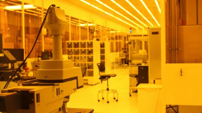
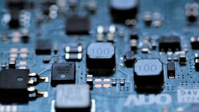
It feels like every day there’s some new tech gadget or update, right? But what’s really making all that possible? It’s the tiny chips inside, the ones that keep getting smaller and smarter. We’re talking about a big jump now, to what they call the 3-nanometer chip. It’s a pretty wild engineering feat, and it means our phones, computers, and all sorts of other devices are about to get a serious upgrade. So, what’s the big deal with these 3nm chips, and how did we even get here?
Key Takeaways
- The 3-nanometer chip represents a significant step in making transistors incredibly small, leading to faster and more energy-efficient electronics.
- Moore’s Law, the idea that computing power doubles about every two years, has been the main driver pushing engineers to shrink chip components.
- New materials and advanced designs like Gate-All-Around transistors are key to making 3nm chips work and pushing beyond this milestone.
- These smaller, faster chips will power big changes in areas like artificial intelligence, the Internet of Things, and healthcare technology.
- Beyond just shrinking, future progress relies on new packaging methods, smart design tools, and global teamwork in the semiconductor industry.
Understanding the 3-Nanometer Chip Revolution
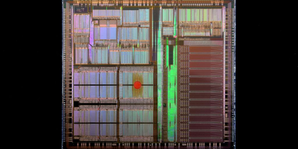
It’s pretty wild to think about how much our world runs on these tiny little things called semiconductors. You know, the chips inside your phone, your laptop, even your smart fridge? They’re basically the brains of all our gadgets. For decades, engineers have been on this quest to make them smaller and smaller, and faster and faster. This whole push is largely thanks to something called Moore’s Law.
The Unseen Hero: Semiconductors and Their Evolution
Semiconductors are materials that can control electricity, kind of like a gatekeeper. Silicon, which we get from sand, is the most common material used. Engineers carve super-tiny pathways onto silicon wafers to create what we call integrated circuits, or microchips. These chips are packed with billions of transistors, which are like tiny switches that flip on and off to process information using ones and zeros. The more transistors you can cram onto a chip, the smarter and quicker your device can be. It’s a constant race to pack more power into less space.
Moore’s Law: The Driving Force Behind Miniaturization
Back in 1965, a guy named Gordon Moore, who helped start Intel, noticed something pretty interesting. He figured out that the number of transistors engineers could fit onto a chip seemed to double about every two years, without making the chips much more expensive. This observation became known as Moore’s Law, and it’s been like a roadmap for the entire tech industry, predicting the incredible growth in computing power we’ve seen. We’ve gone from chips with 90-nanometer transistors in the early 2000s to the 7nm and 5nm chips we see today, and now we’re hitting the 3nm mark. At this scale, transistors are just a few atoms wide!
The Significance of the 3nm Milestone
Hitting the 3-nanometer (nm) process node is a really big deal. It means we can make chips that are not only smaller but also significantly faster and use less power. Companies like Samsung and TSMC are already producing these 3nm chips, and early reports suggest they offer about a 35% performance boost and a 40% reduction in power consumption compared to older generations. This isn’t just a small step; it’s a leap forward that will make our devices quicker, last longer on a single charge, and handle more complex tasks, especially things like artificial intelligence. It’s a testament to how far we’ve come and a sign of even more exciting things to come in the world of computing.
Key Innovations Enabling 3nm Chip Advancement
So, how do we even get to these tiny 3-nanometer chips? It’s not like just shrinking things down with a photocopier. A lot of smart people have been working on some pretty wild ideas to make this happen.
Exploring New Materials for Enhanced Performance
For a long time, silicon was the go-to material for pretty much everything in chips. But as we keep shrinking, silicon alone starts to hit its limits. So, researchers are looking at new stuff. Think about materials like Gallium Arsenide (GaAs) or even combinations of different elements. These aren’t just random choices; they have properties that let electricity move faster or use less power. It’s like finding a better kind of wire for your electrical system. Getting these new materials to work reliably in a manufacturing setting is a huge hurdle, but it’s what allows us to push past the old boundaries.
Advanced Transistor Architectures: Gate-All-Around and FinFETs
Remember those old flat transistors? They’re basically obsolete for cutting-edge chips. We’ve moved on to things like FinFETs, which are like little fins sticking up from the chip surface. This gives the gate, the part that controls the electricity, a much better grip on the current. But even FinFETs are getting a bit crowded at 3nm. The next big thing is Gate-All-Around (GAA) transistors. Imagine wrapping the gate all the way around the channel where the electricity flows. This gives you even finer control, meaning less wasted power and more speed. Samsung and TSMC are both heavily invested in GAA for their 3nm production. It’s a complex manufacturing process, but it’s key to making these smaller, more efficient chips work.
The Role of 3D Integration and Chiplet Designs
Instead of just making everything flatter and smaller on a single piece of silicon, another approach is to stack things up. This is where 3D integration and chiplets come in. Think of it like building a skyscraper instead of just spreading out a ranch house. Chiplets are smaller, specialized pieces of silicon that do specific jobs, and they’re all connected together. This lets companies mix and match different technologies and manufacturing processes. For example, you could have a super-fast processing chiplet made with the latest 3nm tech, connected to a memory chiplet made with a different, optimized process. It’s a way to get more functionality and better performance without having to cram everything onto one impossibly small piece of silicon. This approach is also helping to make advanced computing more accessible, as companies like Intel are exploring new ways to connect these components. The future of chip design is definitely looking more modular and stacked, which is a big change from the old way of doing things. This kind of innovation is what’s driving the next wave of AI capabilities, and it’s fascinating to see how it all comes together. You can see how AI is already helping to speed up chip design processes. AI in chip design
The Impact of 3nm Chips Across Industries
So, what does this whole 3-nanometer chip thing actually mean for us? It’s not just about making phones faster, though that’s part of it. These tiny advancements are like superchargers for a whole bunch of technologies we use every day, and some we haven’t even fully imagined yet.
Revolutionizing Artificial Intelligence and Machine Learning
Artificial intelligence (AI) and machine learning (ML) are hungry for processing power. Think about all the data these systems crunch to recognize faces, understand speech, or even drive cars. With 3nm chips, AI models can become much more complex and learn faster. This means AI could get a lot smarter, a lot quicker. We’re talking about AI that can handle more intricate tasks, leading to better medical diagnoses or more realistic virtual worlds. It’s a big deal for anyone working with big data.
Transforming the Internet of Things and Smart Devices
The Internet of Things (IoT) is all about connecting everyday objects – your fridge, your thermostat, even your toothbrush – to the internet. For these devices to work well, they need to be small, power-efficient, and smart. 3nm chips allow for smaller, more capable processors in these gadgets. This could lead to smarter homes that really anticipate your needs, or industrial sensors that can operate for years on a single battery. Imagine a world where your devices are not just connected, but truly intelligent and low-power.
Advancements in Healthcare and Biotechnology
In healthcare, smaller and more powerful chips can make a huge difference. Think about portable medical devices that can monitor your health in real-time, or advanced imaging equipment that provides clearer results. 3nm technology can help create more sophisticated diagnostic tools and even assist in personalized medicine by processing complex genetic data faster. It’s about making healthcare more accessible and precise.
Enhancing Consumer Electronics and Automotive Technology
For our everyday gadgets, like smartphones and laptops, 3nm chips mean better performance and longer battery life. Apple’s M3 chip, for instance, uses 3nm technology to boost performance for tasks like video editing and gaming, while also extending how long your device lasts on a charge. In cars, these chips can power more advanced driver-assistance systems, better infotainment, and even the complex computations needed for self-driving capabilities. The push for smaller, more efficient chips is directly translating into more capable and user-friendly devices across the board. This constant innovation is what keeps our gadgets feeling fresh and exciting, making everyday tasks smoother and opening up new possibilities for how we interact with technology, much like how future PCs are expected to become more interactive [46b9].
Performance Gains and Future Trajectories
So, what does this whole 3-nanometer thing actually mean for how fast our computers and gadgets can go, and how much power they use? It’s pretty wild when you think about it. We’re talking about packing way more tiny switches, called transistors, into the same space. This means things just get faster, and they don’t need as much juice to run.
Unprecedented Processing Speed and Energy Efficiency
Basically, smaller transistors switch on and off quicker. This translates directly into faster calculations and operations. Imagine your phone processing photos or your laptop rendering video – it’ll happen noticeably quicker. But it’s not just about raw speed. Because these transistors are so small, they also use less electricity. This is a big deal for battery life in everything from your smartwatch to your car. The 3nm process is a major step in making electronics more powerful without draining batteries dry.
Here’s a quick look at what we can expect:
- Speed Boost: Expect significant jumps in processing power, making complex tasks feel much smoother.
- Power Savings: Devices will run longer on a single charge, and the overall energy consumption of electronics will drop.
- More Features: More processing power in a small space means manufacturers can cram more features into devices without making them bigger.
The Path to Sub-Nanometer Technologies
But we’re not stopping at 3 nanometers, are we? Nope. The industry is already looking ahead to 2 nanometers and even smaller. It’s like a race to make things as tiny as possible. This involves figuring out new ways to build these incredibly small components. For instance, researchers are exploring materials beyond traditional silicon, like graphene or carbon nanotubes, which have some pretty neat electrical properties at these tiny sizes. Getting these materials to work reliably in chips is the next big hurdle.
Exploring New Computing Paradigms Beyond Silicon
And what happens when we hit the absolute physical limits of silicon? Well, that’s where things get really interesting. People are looking at entirely different ways to compute. Think about quantum computing, which uses quantum mechanics to solve problems that are impossible for today’s computers. Or neuromorphic computing, which tries to mimic the human brain’s structure. There’s also optical computing, which uses light instead of electricity to process information – some scientists have even managed to get light to travel faster than light on a microchip using special materials, which could really change things up Scientists have achieved faster-than-light speeds on a microchip.
These new approaches might seem like science fiction now, but they’re where the future of computing might be heading once we can’t shrink silicon any further.
The Global Economic and Strategic Importance
Semiconductors as the Backbone of the Digital Economy
Look, it’s pretty obvious that chips are everywhere these days. They’re not just in our phones and computers anymore; they’re in our cars, our refrigerators, even our smart toothbrushes. This massive reliance means the semiconductor industry is basically the engine of the entire global economy. Think about it – without these tiny pieces of silicon, none of our modern tech would work. The market for these things is huge, easily topping hundreds of billions of dollars annually. Getting your hands on the latest, most advanced chips, like the 3-nanometer ones we’re talking about, isn’t just a nice-to-have; it’s a serious competitive edge.
Geopolitical Implications of Chip Manufacturing Dominance
This isn’t just about business anymore; it’s become a major international issue. Countries are pouring money into chip production and research because having control over this technology means having influence. It’s like controlling the oil supply, but for the digital age. Whoever makes the most advanced chips has a significant advantage, not just economically, but strategically. This has led to a lot of tension and competition between nations, as everyone wants a piece of the action and fears being left behind. It’s a real high-stakes game.
Investment and Development in Advanced Chip Production
Because of all this, there’s a massive push for investment. Companies and governments are spending fortunes to build new factories and develop better chip-making techniques. It’s a race to stay ahead, and the costs are astronomical. We’re seeing new materials and manufacturing processes being explored, all aimed at pushing the boundaries of what’s possible. This intense focus on development is what’s driving innovations like the 3nm chip revolution, but it also means that only the biggest players with the deepest pockets can really compete at this level. It’s a tough environment for smaller companies trying to break in.
Sustaining Progress: Design, Packaging, and Collaboration
The Critical Role of Semiconductor Packaging Innovations
So, we’ve talked a lot about how tiny we can make the actual transistors, right? Like getting down to 3 nanometers. But here’s the thing: as chips get smaller and more powerful, how we package them becomes just as important. It’s like having a super-fast engine, but if you put it in a flimsy car body, it’s not going to work well. Packaging is basically how the chip is housed and connected to everything else in a device. Think about 3D packaging, where chips are stacked on top of each other. This lets us pack more power into a smaller space, which is a big deal for things like smartphones or even those tiny sensors in medical equipment.
Leveraging AI and Machine Learning in Chip Design
It’s not just about making the chips themselves; it’s also about how we design them. This is where AI and machine learning are really starting to shine. Designing these complex chips used to take ages, with engineers trying out tons of different layouts. Now, AI can help speed that up a lot. It can look at millions of possibilities for how to arrange components on a chip to get the best performance and use the least power. This is super helpful when you’re trying to hit those tight power, performance, and area (PPA) targets, especially for AI applications. It’s like having a super-smart assistant that can crunch numbers and find the best design much faster than a human could.
The Importance of Global Collaboration in Semiconductor Advancement
Finally, none of this happens in a vacuum. Making these cutting-edge chips, especially as we push towards even smaller sizes like 1 or 2 nanometers, needs everyone to work together. We’re talking about chip makers, research labs, and even the companies that build the machines used to make the chips. For example, getting the right tools for things like Extreme Ultraviolet (EUV) lithography, which is what lets us print those super-fine lines on chips, required a huge effort between different companies. Plus, as we face challenges like heat dissipation and quantum effects at these tiny scales, sharing knowledge and working across borders is really the only way to find solutions. It’s a global effort, for sure.
The Journey Continues
So, we’ve seen how these tiny 3-nanometer chips are a pretty big deal. They’re making our gadgets faster and use less power, which is great for everything from our phones to big computer systems. But this isn’t the end of the road. The people working on this stuff are already looking at even smaller sizes, like 2-nanometer chips and beyond. It’s not just about making things smaller, though. They’re also figuring out new ways to design chips, using different materials, and working together across the globe. This whole semiconductor thing is really just getting started, and it’s going to change our future in ways we can’t even imagine yet.
Frequently Asked Questions
What exactly are nanometer chips?
Think of nanometer chips as the tiny brains inside our electronic gadgets. They’re made of a special material that lets electricity flow through them in a controlled way. Engineers carve super-tiny paths on these chips, like roads for electricity, to make them do all the thinking and remembering for our phones, computers, and more. The smaller the nanometer number, the more of these tiny paths, called transistors, can fit on one chip, making it faster and smarter.
What is Moore’s Law and why is it important for these chips?
Moore’s Law is like a prediction made a long time ago that said the number of tiny parts, called transistors, on a chip would double about every two years. This has been a guiding rule for chip makers, pushing them to make chips smaller and more powerful without making them too expensive. The 3-nanometer chip is a big step in following this rule, showing that we can still make chips much smaller and better.
Why is the 3-nanometer chip a big deal?
Reaching the 3-nanometer size is a huge achievement because it means chips can be much faster and use way less power. Imagine your phone lasting much longer on a single charge or your computer running complex programs without getting hot. These chips make devices quicker, more efficient, and allow for amazing new technologies like advanced artificial intelligence and super-fast internet.
What new technologies are helping us make these tiny 3nm chips?
Making chips this small is tricky! Scientists are using new materials that work better than older ones, and they’ve invented new ways to build the tiny switches (transistors) called Gate-All-Around. They’re also stacking these chips on top of each other, like building a tiny skyscraper, to fit even more power into a small space. Plus, they’re using smart computer programs, like artificial intelligence, to help design and build them perfectly.
How will 3nm chips change the world?
These super-fast and efficient chips will make a big difference everywhere! Artificial intelligence will get much smarter, helping us with everything from driving cars to understanding diseases. Our smart devices, like watches and home assistants, will work better and last longer. In medicine, they’ll help create new ways to monitor health and develop treatments. Basically, anything that uses electricity will get a major upgrade.
Are companies already making 3nm chips, and what’s next?
Yes, some companies have already started making 3-nanometer chips, and they’re powering the latest gadgets. But the work doesn’t stop there! Engineers are already thinking about even smaller chips, like 2-nanometer ones, and exploring completely new ways to compute, maybe even using things like quantum mechanics. They’re also looking at new materials and better ways to put chips together to keep making our technology better and better.


