Have you ever wondered about the journey of the integrated circuit package? It’s gone through so many changes over the years, and it’s still evolving! From the very first designs to the super small ones we see in our phones today, the integrated circuit package has a pretty cool story. This article will walk you through its history, what made it change, and what we might see next in this important piece of technology.
Key Takeaways
- The integrated circuit package started with simple designs like the Dual In-Line Package, then moved to surface mount tech, and now uses area array packages for more connections.
- The main reasons integrated circuit packages changed were the need for more connections, smaller sizes for mobile devices, and better cost and performance.
- As chips got more complex, the integrated circuit package had to handle more connections, leading to things like Pin Grid Array and Ball Grid Array designs, and then tiny Chip Scale Packages.
- The demand for smaller gadgets pushed the integrated circuit package to shrink, with innovations like Quad Flat No-Leads and super-compact Wafer Level Chip Scale Packages.
- Looking ahead, the integrated circuit package is moving towards combining different technologies in one unit, using 3D stacking to make things even smaller and more powerful.
Historical Milestones in Integrated Circuit Package Development
IC packaging has come a long way! It’s wild to think about how much things have changed since the first IC packaging was introduced. Let’s take a quick look at some of the big moments that shaped how we package chips today.
The Dawn of Dual In-Line Packages
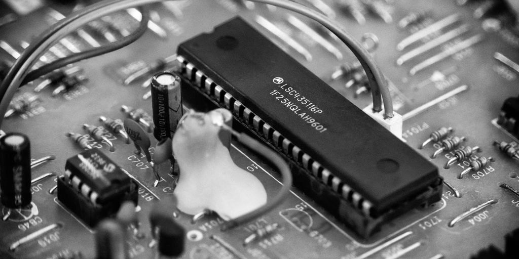
Back in the 1960s, some engineers at Fairchild came up with the Dual In-Line Package (DIP). This was a game-changer. It was basically the first real semiconductor package, with two rows of pins sticking out. The DIP became super popular in the 70s. It was easy to use and made things a lot simpler for circuit board design. It’s amazing to think that something so simple had such a big impact.
Emergence of Surface Mount Technology
Fast forward to the early 1980s, and we see the rise of surface mount packaging. Instead of sticking pins through holes in a board, these components could be soldered directly to the surface. This meant smaller boards and more automated assembly. It was a big step towards the compact electronics we have today. It also paved the way for more complex designs.
Evolution of Area Array Packages
Then came area array packages. These were different because they didn’t just use the edges of the package for connections. Instead, they spread the connection points across the entire surface. Think of Ball Grid Arrays (BGAs) and Pin Grid Arrays (PGAs). This allowed for way more connections than before. It was a huge deal for chips that needed a ton of input/output connections.
Driving Forces Behind Integrated Circuit Package Evolution
The Quest for Higher Pin Counts
So, why did we need more pins on these IC packages anyway? Well, it all boils down to needing more connections. Think of it like this: the more pins, the more data can flow in and out of the chip. This was especially important for high-end systems used in computers, networking gear, and storage devices. They needed to move a ton of data quickly. Finding the sweet spot between size, how much power it used, and cost was a big challenge. That’s what led to the development of Pin Grid Array (PGA) and Ball Grid Array (BGA) packages, which are still around today. Initially, these used ceramic, but now laminates are more common because they’re cheaper. Then, in the 90s, when even more pins were needed, the Chip Scale Package (CSP) came along. It’s basically a smaller BGA, with the balls packed closer together. This helped accommodate increased input/output connections.
Miniaturization for Mobile Devices
Remember those huge cell phones from the 80s? Nobody wants those anymore! The 90s saw a big push to make everything smaller, especially for laptops and cell phones. These devices needed packages that were about the same size as the chips themselves. This also helped keep costs down. One of the big wins here was the Quad Flat No-leads (QFN) package. It’s a type of Chip Scale Package (CSP) and it became super popular because it was simple, worked well, and didn’t cost a fortune. Another cool thing that came out of this was the Wafer Level Chip Scale Package (WLCSP), also called a bumping package. It’s about as small as you can get, since the package is basically the same size as the die itself. The introduction of the Quad Flat No-leads (QFN) package was a game changer.
Cost-Effectiveness and Performance Optimization
Ultimately, it’s always a balancing act. You want the package to perform well, but you also need it to be affordable. No one wants to pay a fortune for a chip package, no matter how amazing it is. So, engineers are constantly looking for ways to get the best bang for their buck. This means finding materials and designs that are cheap to make but still do the job. It also means optimizing the package to get the best possible performance out of the chip. This involves things like reducing resistance and capacitance, and making sure the heat can get away from the chip easily. Here’s a quick look at how package tech evolved over time:
| Decade | Major IC Packaging Inventions |
|---|---|
| 1970s | Dual In-Line Package (DIP), Ceramic Integrated Circuit Package (ICP), Quad Flat Package (QFP), Small Outline Package (SOP), Leadless Chip Carrier (LCC) |
| 1980s | Surface Mount Packages, Area Array Packages |
| 1990s | Chip Scale Packages (CSPs), Quad Flat No-Leads (QFN) |
| 2000s-2010s | System-in-Package (SiP), Package-on-Package (PoP) |
| 2020+ | Multi-Chip Modules (MCMs), 3D SoCs |
This constant drive for better performance at a lower cost is what keeps integrated circuit packaging technologies evolving.
Advancements in Integrated Circuit Package Pin Counts
As chips got more complex, they needed more ways to connect to other components. This led to some cool innovations in how IC packaging was done. It’s all about getting more pins (those little metal legs or balls) onto the package so the chip can talk to the outside world.
Accommodating Increased Input/Output Connections
The need for more input/output (I/O) connections was a big driver in package evolution. Think about it: a chip with a million gates needs a way to get all that data in and out! Early on, packages just didn’t have enough pins to handle it. This is where new designs came into play, focusing on maximizing the number of connections possible.
The Rise of Pin Grid Array and Ball Grid Array
To solve the pin problem, engineers came up with Pin Grid Arrays (PGAs) and Ball Grid Arrays (BGAs). Instead of just having pins around the edges, these packages used the entire bottom surface. PGAs have pins that you stick into a socket, while BGAs have little solder balls that melt and connect to the board. Ball grid array packages really took off in the 90s, especially the flip-chip versions (FCBGA).
Chip Scale Packages for Compact Designs
But what about smaller devices? That’s where Chip Scale Packages (CSPs) came in. The goal was to make the package as close to the size of the chip itself as possible. This was super important for things like cell phones and laptops. One popular type of CSP is the Quad Flat No-leads (QFN) package. It’s simple, performs well, and doesn’t cost a fortune. Another advancement was the Wafer Level Chip Scale Package (WLCSP), which is about as small as you can get, since the ceramic Dual-in-Line Package dimensions are basically the same as the chip itself. These advancements really helped with miniaturization. The table below shows the evolution of IC packaging by decade:
| Decade | Major IC Packaging Inventions |
|---|---|
| 1970s | Dual In-line Package (DIP), Ceramic Integrated Circuit Package (ICP), Quad Flat Package (QFP), Small Outline Package (SOP), Leadless Chip Carrier (LCC) |
| 1980s | Surface mount packaging |
| 2020+ | MCMs, 3D SoCs |
The Push for Smaller Integrated Circuit Package Sizes
The 1990s marked a turning point with a major push for miniaturization in IC packaging. This was largely fueled by the boom in mobile devices like laptops and cell phones, which demanded smaller, more compact packages. The goal was to reduce both the package cost and the overall footprint of the device.
Meeting Demands of Portable Electronics
Portable electronics set a new bar for package size. The race was on to create packages that were as close as possible to the size of the IC itself. This wasn’t just about making things smaller; it was about making devices more efficient and portable. Think about how much smaller phones have gotten over the years – a lot of that is thanks to advances in IC packaging.
Quad Flat No-Leads Package Innovations
One of the key innovations to come out of this push was the Quad Flat No-Leads (QFN) package. QFN packages quickly became popular because they were simple, performed well, and were cost-effective. They fall under the category of Chip Scale Packages (CSPs). Here’s a quick look at why QFNs were such a hit:
- Simplicity in design and manufacturing.
- Good thermal performance.
- Small footprint.
Wafer Level Chip Scale Package for Ultimate Miniaturization
For the ultimate in miniaturization, the Wafer Level Chip Scale Package (WLCSP), also known as the bumping package, emerged. This package is considered the smallest because its dimensions are practically the same as the die itself. It’s like the IC is wearing a super-thin skin. WLCSP really pushed the boundaries of what was possible, allowing for incredibly compact designs. The evolution of ceramic Dual-in-Line Package (DIP) to WLCSP is a wild ride!
Integrated Circuit Package Evolution into Heterogeneous Integration
Moore’s Law has been a driving force, but we’re bumping into limits with traditional 2D scaling. That’s where heterogeneous integration comes in, basically stacking different technologies to get more density and functionality.
Beyond Moore’s Law with 3D Techniques
Instead of just shrinking transistors on a single plane, 3D techniques let us stack multiple layers of silicon. Think of it like building up instead of out. This opens up a lot of possibilities for cramming more performance into a smaller space. It’s not just about stacking the same thing; it’s about mixing and matching different types of devices. For example, you can use 3D techniques to stack memory on top of a processor, which drastically reduces the distance data needs to travel.
Integrating Diverse Technologies in a Single Package
Heterogeneous integration is all about bringing together different components – logic, memory, sensors, even antennas – into one package. This is driven by the need for better power efficiency, higher performance, smaller size, and lower cost. It’s like creating a mini-system on a single chip package. This approach uses interposer technologies and even wire-bonding to connect everything. It’s a complex process, but the payoff is significant.
Future of Denser and Optimized Integrated Circuit Packages
Looking ahead, heterogeneous integration is going to be a key part of future chip design. We’ll see even denser and more optimized packages that combine different materials and technologies. This will enable new levels of performance and functionality in everything from mobile devices to high-performance computing. The advancements in IC packaging will allow for more complex systems to be integrated into smaller spaces. It’s an exciting time for the industry, with lots of innovation happening in this area.
Key Integrated Circuit Package Technologies by Decade
It’s interesting to look back and see how integrated circuit package tech has changed over time. Each decade brought new innovations, driven by the need for more functionality, smaller sizes, and better performance. Let’s take a quick trip down memory lane.
1970s: Foundational Package Inventions
The 1970s were really the starting point for modern IC packaging. This decade saw the invention of several foundational package types that are still recognizable today. The ceramic Dual-in-Line Package (DIP) was a big deal, offering a practical way to connect ICs to circuit boards. Other important packages from this era include the Quad Flat Package (QFP), Small Outline Package (SOP), and Leadless Chip Carrier (LCC).
1980s: Surface Mount and Array Package Innovations
The 1980s brought about a shift towards surface mount technology (SMT). Instead of sticking components through holes in the board, SMT allowed them to be placed directly on the surface. This led to smaller and more efficient designs. The LTCC and HTCC Market really took off. Key innovations included the Pin Grid Array (PGA) and Ball Grid Array (BGA), which allowed for a higher density of connections compared to previous packages.
1990s: Chip Scale and No-Leads Package Advancements
In the 1990s, the focus shifted towards miniaturization, driven by the growing popularity of portable devices. This led to the development of chip-scale packages (CSPs), which were almost the same size as the silicon die itself. The Quad Flat No-Leads (QFN) package also gained traction, offering a compact and cost-effective solution for many applications. These ball grid array (BGA) packages were a game changer.
Modern Integrated Circuit Package Solutions
Integrated circuit (IC) packaging has come a long way, and today’s solutions are pretty impressive. We’re talking about technologies that allow for more functionality in smaller spaces, and that’s a big deal for everything from smartphones to high-performance computers. Modern IC packaging is all about maximizing performance while minimizing size and cost.
System-In-Package and Package-on-Package
System-in-Package (SiP) is a big deal because it lets you put a bunch of different components into one package. Think of it like a mini-motherboard. You can have the processor, memory, and other stuff all in one place. Package-on-Package (PoP) is similar, but it stacks packages on top of each other. This is great for saving space, especially in mobile devices. It’s like building a skyscraper for your electronics.
Here’s a quick rundown of the benefits:
- Increased integration
- Reduced board space
- Improved performance
Wafer-Level Packaging and 2.5D/3D ICs
Wafer-Level Packaging (WLP) is where the packaging is done while the chips are still on the wafer. This makes the final package super small. Then you have 2.5D and 3D ICs, which are all about stacking chips either side-by-side (2.5D) or on top of each other (3D). This lets you pack a ton of functionality into a tiny space. It’s like going from a regular house to a multi-story apartment building. These technologies are key for advanced semiconductor packaging and are becoming more common as we need more power in smaller devices.
Multi-Chip Modules and Advanced Stacking
Multi-Chip Modules (MCMs) are like SiPs, but they often involve putting multiple chips onto a single substrate. This is useful when you want to combine different technologies or have a custom solution. Advanced stacking takes this even further, allowing for complex arrangements of chips and other components. It’s all about getting the most out of the available space and improving performance. Think of it as building a custom Lego set, but for electronics. The evolution of interposer technologies and wire-bonding techniques are also important here.
Here’s a simple comparison:
| Feature | MCM | Advanced Stacking |
|---|---|---|
| Chip Placement | On a substrate | Stacked vertically and horizontally |
| Complexity | Relatively simpler | More complex |
| Use Cases | Combining different technologies | High-density, high-performance systems |
| Space Efficiency | Good | Excellent |
Conclusion
So, we’ve taken a trip through the history of IC packaging, right? It’s pretty wild how much things have changed, from those early, simple designs to the super complex stuff we see today. The constant push for more connections and smaller sizes really shaped everything. And now, with all the talk about putting different kinds of chips together in one package, it feels like we’re just getting started. The future of these tiny powerhouses is going to be interesting, that’s for sure. It’s all about making things faster and more efficient, and packaging is a big part of that story.
Frequently Asked Questions
What exactly is IC packaging?
IC packaging is like the protective shell and connector for the tiny computer chips inside our gadgets. It keeps them safe and helps them talk to other parts of the device.
How have IC packages changed over time?
Early packages, like the Dual In-Line Package (DIP), had pins sticking out the sides. Then came Surface Mount Technology (SMT), where parts sat right on the board. Later, Area Array Packages, like BGAs, used the whole bottom of the chip for connections, allowing for many more connections.
Why do IC packages need more and more connections?
As chips became more powerful, they needed more connections to send and receive information. This led to packages like Pin Grid Array (PGA) and Ball Grid Array (BGA) that could handle many more connections.
What made IC packages get so much smaller?
With phones and other portable devices, everything needed to shrink. This pushed for smaller packages like Quad Flat No-Leads (QFN) and Wafer Level Chip Scale Packages (WLCSP), which are super tiny, almost the size of the chip itself.
What does ‘heterogeneous integration’ mean for IC packages?
Heterogeneous integration means putting different types of chips or parts together in one package, even if they weren’t originally designed to work side-by-side. Think of it like building a super-device by combining different specialized blocks.
What’s next for IC packaging?
In the future, we’ll see even more advanced ways to stack chips and combine different technologies within a single package. This will lead to even more powerful and compact electronic devices.