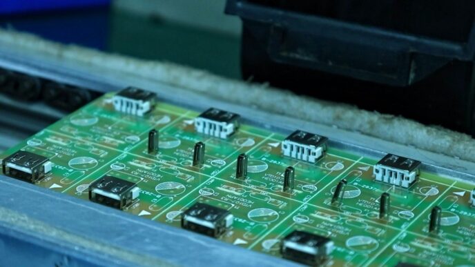
Chip manufacturing is always changing, and the latest big thing is something called hyper-NA EUV. It’s a new way to use light to make super tiny patterns on computer chips. Think of it like a super-powered magnifying glass for making the smallest parts of electronics we’ve ever seen. This technology is a big deal because it could lead to much faster and more efficient computers and gadgets, especially for things like artificial intelligence. We’re going to look at how this hyper-NA EUV tech works, why it’s important, and what it means for the future of making chips.
Key Takeaways
- Hyper-NA EUV, with its 0.7 numerical aperture, is the next step in EUV lithography, aiming to support the creation of 1nm chip nodes.
- The demand for AI processing power is a major reason why companies are investing heavily in EUV technology, including the upcoming hyper-NA EUV.
- Advancements in light source power, precision droplet control, and debris management are making EUV systems more effective.
- Geopolitically, Asia-Pacific is leading in EUV production, while countries like China are pushing for self-sufficiency, and North America is focusing on bringing manufacturing back.
- While hyper-NA EUV promises significant improvements, the cost of these advanced systems is expected to be substantial, following the trend of increasing prices with each new generation of EUV.
The Evolution of EUV Lithography
It feels like just yesterday we were talking about how amazing Extreme Ultraviolet (EUV) lithography was, and now, here we are, already looking at the next big leap. ASML, the company that pretty much everyone relies on for these machines, has been steadily improving its EUV systems. It’s a bit like how phone cameras get better every year, but way, way more complicated and expensive.
0.3 NA EUV: The Foundational Step
This was the starting point, the first real push into using EUV light for making chips. With a numerical aperture (NA) of 0.3, it was a big deal because it actually worked and showed that EUV could be a thing. But, honestly, it had its limits. The resolution wasn’t good enough for the really tiny features we need today, so it was more of a stepping stone than the final answer. Think of it as the first smartphone – it made calls, but it didn’t do much else.
0.55 High NA EUV: Enhanced Resolution
Next up was the High NA EUV, bumping the numerical aperture to 0.55. This was a pretty significant jump. This improvement allowed for much finer detail, letting chipmakers pack more transistors onto a single chip. Companies like Intel, TSMC, and Samsung started getting these systems to make chips for the 2nm node, aiming for around 2025. It’s a big step up, but as you might guess, these machines cost a fortune – we’re talking hundreds of millions of dollars each. It’s a bit like upgrading from a basic car to a sports car; you get a lot more performance, but the price tag is considerably higher. The market for these advanced systems is growing fast, with projections showing it could reach over $26 billion by 2030, largely thanks to the demand for AI chips. You can see how the technology is progressing by looking at the evolution of 3D printing – different stages, each building on the last.
0.7 Hyper NA EUV: The Next Frontier
And now we’re talking about Hyper NA EUV, aiming for a 0.7 numerical aperture. This is where things get really interesting for the future, like the 1nm node and beyond. It’s still in the early stages of development, but the goal is to push resolution limits even further. This kind of tech is what’s needed to keep up with the demands of AI, which needs incredibly dense chips. It’s not just about making chips smaller; it’s about making them smarter and more powerful. The cost is going to be even higher, of course, but the potential payoff in terms of computing power is massive. It’s a bit like trying to build a supercomputer in your garage – incredibly difficult and expensive, but the possibilities are mind-blowing.
Hyper NA EUV: Enabling Future Chip Nodes
So, we’ve talked about the older EUV stuff, but what’s next? Well, it’s all about getting even more precise, and that’s where Hyper NA EUV comes in. Think of it as upgrading from a regular camera lens to a super-telephoto zoom – you can see and do so much more.
Pushing Resolution Limits with 0.7 NA
This new generation, often called Hyper NA EUV, is aiming for a numerical aperture (NA) of 0.7. For us regular folks, that means it can draw much, much finer lines on silicon wafers. We’re talking about features that are incredibly tiny, way smaller than what we could do before. This isn’t just a small tweak; it’s a big leap forward in how detailed our chips can get. The goal is to make chips that are not only smaller but also way more powerful and energy-efficient. It’s like going from a basic sketch to a photorealistic drawing, all on the same tiny chip surface.
Supporting 1nm Node Manufacturing
What does this mean for the future? Well, the big buzzword is the ‘1nm node’. While we’re still working out the exact definition and timeline, Hyper NA EUV is being developed specifically to make manufacturing at these incredibly small scales possible. Right now, companies like TSMC are pushing the limits with their current EUV machines, but to get to 1nm and beyond, this new tech is pretty much a requirement. It’s going to be the tool that lets us build the next generation of processors, the ones that will power things we can only dream of today, maybe even helping with things like advanced virtual reality headsets [a839].
Revolutionizing Nano-Fabrication
This isn’t just about making existing chips better; it’s about enabling entirely new ways of designing and building them. With Hyper NA EUV, we can pack more transistors into the same space, which is the classic way Moore’s Law has worked. But it also opens doors for more complex chip designs, like those ‘chiplets’ we’re hearing about, where different parts of a processor are made separately and then put together. This approach lets engineers use the best manufacturing process for each specific part, rather than trying to cram everything onto one giant, complicated chip. It’s a whole new ballgame for how we think about making electronics.
Market Dynamics and Growth Drivers
It’s pretty wild how fast the whole EUV lithography scene is growing. We’re talking about a market that was around $10 billion in 2024 and is expected to hit nearly $27 billion by 2030. That’s a huge jump, right? A lot of this is thanks to the massive demand for AI chips. Think about it, chips for AI need way more of these EUV-patterned layers than older chips. Nvidia’s H100 GPUs, for instance, use about five times more EUV layers than standard chips. That really shows how important this tech is becoming.
Governments are also pouring money into this. The US CHIPS Act, the EU Chips Act, and similar programs in India are all about building up semiconductor manufacturing. It’s like everyone wants their own reliable chip supply. Plus, there’s the energy efficiency angle. Chips made with EUV at smaller nodes use a lot less power. For data centers and all that cloud computing, saving energy means saving a ton of money.
AI Demand Fueling EUV Adoption
Artificial intelligence is really the big driver here. As AI models get more complex, they need more powerful processors. These processors, in turn, require the incredibly fine details that only EUV lithography can provide. It’s a direct link: more AI development means more demand for the most advanced chips, which means more demand for EUV machines. We’re seeing companies invest heavily in EUV to keep up with the pace of AI innovation. It’s a bit of a race to build the best AI hardware.
Government Investments in Semiconductor Ecosystems
Governments worldwide are recognizing that having a strong domestic semiconductor industry is a matter of national security and economic competitiveness. That’s why we’re seeing these huge investment packages. The goal is to reduce reliance on foreign manufacturing and build resilient supply chains. These investments cover everything from research and development to building new factories, or fabs. It’s a long-term strategy to ensure access to the chips that power everything from our phones to our defense systems. This also helps create jobs and boost local economies. It’s interesting to see how different countries are approaching this, like China’s push for self-reliance or North America’s reshoring efforts. You can even see how companies like Intel are getting involved, like their big investment in a new fab in Ohio. It’s all part of a bigger global shift.
Energy Efficiency Gains with Advanced Nodes
When you shrink down the transistors on a chip, they generally use less power. EUV lithography is key to making these smaller, more efficient chips. For example, chips made using EUV at the 3nm node can use up to 30% less power than older chips made at 7nm. This might not sound like much on a single chip, but when you’re talking about massive data centers with thousands of servers, or even just your smartphone battery life, those savings add up fast. It means less electricity consumption and less heat generated, which is a big deal for performance and sustainability. It’s a win-win, really. This push for efficiency is also driving the development of new materials, like zero-index materials that allow light pulses to travel incredibly fast on a microchip, potentially revolutionizing computer processing.
Here’s a quick look at some of the major government initiatives:
- United States: CHIPS and Science Act (over $52 billion)
- European Union: EU Chips Act (around €43 billion)
- India: Semiconductor Mission (approximately $10 billion)
These aren’t small numbers, and they show how serious governments are about securing their semiconductor future. It’s a global effort, and the competition is definitely heating up.
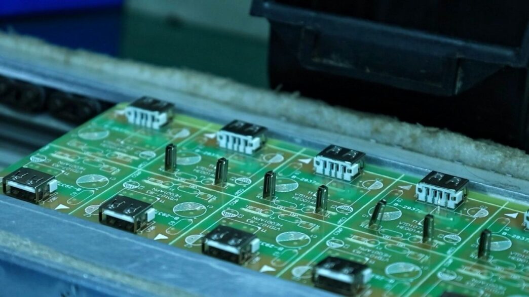
Technological Advancements in EUV
It’s pretty wild how much work goes into making these tiny chips, right? EUV lithography, especially the newer stuff, is a whole different ballgame. They’re constantly tweaking and improving the machines to get even better results.
Innovations in Light Source Engineering
The heart of any EUV system is its light source. Think of it as the super-powered flashlight that etches the patterns. The current go-to is something called Laser-Produced Plasma (LPP). Basically, they blast a tiny droplet of tin with a powerful laser, and that creates a super-hot plasma that emits EUV light. The goal here is to make that light source stronger and more consistent. We’re seeing LPP systems hitting power levels of around 500 watts now, which is pretty impressive. This higher power means the machines can process more silicon wafers per hour, which is a big deal for keeping up with demand. To make this work, the tin droplet targeting has to be incredibly precise, down to fractions of a nanometer. It’s like trying to hit a moving target with a laser pointer from miles away, but way, way smaller.
Precision in Droplet Generation Systems
Speaking of those tin droplets, getting them just right is a whole engineering challenge. These systems need to produce incredibly uniform droplets, and they have to be in the exact right spot when the laser hits them. We’re talking about targeting accuracy within 0.1 nanometers. If a droplet is even a little bit off, or not the right size, it can mess up the light output. This precision is what allows the EUV scanners to keep up a good pace, aiming for over 200 wafers processed every hour. It’s a delicate dance between fluid dynamics and laser control.
Advanced Debris Mitigation Techniques
One of the big headaches with EUV is something called "debris." When the tin plasma is created, tiny bits of tin can fly off and stick to the mirrors and lenses inside the machine. This gunk can block the EUV light or even damage the optics over time. So, engineers have come up with clever ways to deal with this. They use special "pellicles," which are super-thin membranes that protect the most sensitive optics, and they also have systems to clean or deflect any stray particles. These improvements are pretty significant, helping to keep the machines running smoothly and reducing downtime. We’re seeing productivity gains of about 30% thanks to these debris control methods, which really adds up when you’re talking about manufacturing millions of chips. It’s all about keeping those expensive machines running as much as possible, and these advancements are key to that. The ongoing work in EUV lithography is really what’s enabling new possibilities, pushing the boundaries of what’s achievable in chip production pushing the boundaries of what’s achievable in chip production.
Geopolitical and Regional Shifts in EUV
The global semiconductor manufacturing landscape, especially concerning EUV lithography, is really shifting. It’s not just about who has the best tech anymore; it’s about national strategies and economic power.
Asia-Pacific’s Dominance in EUV Production
Right now, Asia-Pacific is where most of the EUV action is happening. Taiwan, thanks largely to TSMC, is a huge player, holding a significant chunk of the EUV market. TSMC’s massive investments in new chip manufacturing facilities really cement this position. They’re pushing ahead with the latest nodes, and it looks like they’ll keep setting the pace for a while. From 2024 to 2029, the EUV segment in Taiwan is expected to grow quite a bit, faster than in many other parts of the world.
China’s Drive for Technological Self-Reliance
Meanwhile, China is on a mission to build its own semiconductor capabilities. They’re facing restrictions on getting the most advanced EUV systems from places like ASML, but their domestic EUV market is still growing, and at a pretty fast clip too. A lot of this is thanks to substantial government funding aimed at creating a self-sufficient chip supply chain. It’s a big push for independence in a critical technology sector.
North America’s Strategic Reshoring Initiatives
Over in North America, there’s a clear focus on bringing chip manufacturing back home. Big investments in new fabs, supported by government programs like the CHIPS and Science Act, are expected to boost the region’s EUV market significantly by 2030. These moves show a broader global trend of countries trying to secure their own semiconductor production and technological future. It’s a complex web of national interests and technological advancement, and it’s changing where and how these advanced chips get made. The outlook for ASML’s revenue, for instance, is being watched closely amidst these geopolitical shifts, with the company cautioning about potential stagnation due to increasing risks [3e49].
Cost Considerations for Hyper NA EUV
So, let’s talk about the price tag for this new Hyper NA EUV gear. It’s no secret that this kind of advanced tech doesn’t come cheap. We’ve seen the costs climb with each step up in EUV capability.
Historical Cost Trends of EUV Systems
When ASML first rolled out the 0.3 NA EUV machines, they were around $200 million a pop. That was a big deal back then, a huge investment for any chipmaker. Then came the 0.55 High NA EUV systems, and the price jumped up to about $380 million. That’s nearly double, reflecting the added complexity and the push for better resolution. It’s like going from a decent sedan to a high-performance sports car – you pay for the advanced engineering.
Factors Influencing Hyper NA EUV Pricing
Now, for the Hyper NA EUV, which aims for a 0.7 NA, we’re looking at even more advanced optics and systems. Think about it: more precise mirrors, more complex light sources, and tighter tolerances all around. These things add up. Plus, the research and development costs to get to this point are massive. The sheer technological leap required for 0.7 NA means the initial price will likely be significantly higher than the $380 million for the High NA systems. We’re talking about pushing the absolute limits of what’s possible in optics and precision engineering.
Economies of Scale and Market Dynamics
Of course, as ASML makes more of these Hyper NA machines, the cost per unit should eventually come down. That’s just how manufacturing works – economies of scale. But it’s going to take time and a lot of demand. The market for these machines is pretty specialized, mostly big chip manufacturers who need the absolute cutting edge for their most advanced chips. Government investments and the booming demand for AI chips are definitely pushing companies to adopt this tech, but the upfront cost is still a major hurdle. It’s a balancing act between the incredible capabilities these machines offer and the very real financial investment required.
Complementary Lithography Techniques
While Hyper NA EUV is definitely the shiny new thing, it’s not like older technologies are just going to disappear. The semiconductor world is all about making the most of what you have, and that means finding ways to keep older tools relevant for as long as possible. Think of it like keeping your old reliable car running even after you buy a new sports car – you still need it for certain trips, right?
One big area is how we use existing 193nm Deep Ultraviolet (DUV) lithography. This has been the workhorse for years, and the industry has gotten incredibly good at pushing its limits. Techniques like multi-patterning, where you essentially print a pattern multiple times to create finer features, are still super important. We’re talking about methods like self-aligned double patterning (SADP) and even quadruple patterning (SAQP). These rely heavily on precise spacer deposition, often using atomic layer deposition (ALD), to control the critical dimensions. It’s a bit like using stencils multiple times to build up a complex image.
Then there’s this idea of curvilinear masking. Normally, the patterns on a mask are all straight lines, like city blocks. Curvilinear masking allows for more curved, organic shapes. This can actually help expand the ‘process window,’ which is basically the range of conditions where the chip-making process works reliably. It’s not strictly necessary for older nodes, but for the smaller ones, it’s becoming quite useful. The development of multi-beam mask writers has made these curvy masks more practical to create without breaking the bank. It’s a way to get more out of the mask itself, and the cost increase is pretty small compared to, say, buying a whole new EUV machine.
We also can’t forget about other methods that aren’t strictly lithography but work alongside it. Directed self-assembly (DSA) is one. It’s not really for printing patterns from scratch yet, but it’s great for fixing minor imperfections in patterns that lithography creates, like smoothing out rough lines or filling in tiny gaps. It’s more of a ‘pattern healing’ process right now. Some folks are looking at pattern multiplication with DSA, but honestly, the industry has gotten so good at using spacers for that, DSA has a tough road ahead in that specific application. Still, for fixing things, it’s pretty neat.
It’s all about a layered approach. You’ve got your cutting-edge Hyper NA EUV for the absolute smallest features, but you’re still going to see 193nm DUV, multi-patterning, and clever mask designs working together. It’s how the industry keeps innovating and making more powerful chips without needing a completely new toolkit for every single step. For a deeper look at these foundational processes, you can check out this resource on essential lithography techniques essential lithography techniques.
What’s Next?
So, where does all this leave us? Hyper-NA EUV is a big deal, no doubt about it. It’s pushing chip manufacturing into a whole new zone, making things smaller and faster than we thought possible. This isn’t just about making better phones or computers; it’s about powering the next wave of AI and all sorts of tech we haven’t even dreamed of yet. While the costs are going up and the tech is getting more complex, the industry seems ready to keep investing. It’s a bit like a race, with everyone trying to get ahead. We’ll have to see how it all plays out, but one thing’s for sure: the future of chips is looking pretty wild.
Frequently Asked Questions
What is Hyper NA EUV and why is it important?
Hyper NA EUV is the next big step in chip-making technology. Think of it like a super-powered magnifying glass for printing tiny patterns on computer chips. It uses a special kind of light and lenses with a higher ‘numerical aperture’ (NA) to make even smaller and more detailed designs. This is crucial for creating the super-fast and efficient chips needed for things like advanced artificial intelligence (AI).
How is Hyper NA EUV different from older EUV technologies?
Older EUV systems, like the 0.3 NA and 0.55 High NA versions, were already big improvements. But Hyper NA EUV, with its even higher NA (around 0.7), can print much finer lines and smaller features. This means we can pack more transistors onto a chip, making them more powerful and energy-efficient. It’s like going from a standard pencil to a super-fine technical pen for drawing.
What kind of chips will benefit from Hyper NA EUV?
This advanced technology is mainly for the most cutting-edge computer chips, like those used for AI, supercomputers, and next-generation smartphones. It’s designed to help create chips that are smaller, faster, and use less power, pushing the boundaries of what’s possible in electronics.
Is Hyper NA EUV very expensive?
Yes, these machines are incredibly expensive, costing hundreds of millions of dollars each. Developing this technology also requires massive investments. While the cost is high, the goal is to make future chips more powerful and efficient, which can justify the expense for companies making the most advanced products.
Are there other ways to make small chip patterns besides EUV?
While EUV is leading the way for the smallest features, other methods are still important. For example, older ‘Deep Ultraviolet’ (DUV) technology is still used for many chips and is being improved with techniques like ‘Inverse Lithography Technology’ (ILT) to get more out of it. Also, some companies are looking at different approaches like ‘nanoimprint lithography’.
Who is making this new Hyper NA EUV technology?
The company ASML, based in the Netherlands, is the main leader in developing and manufacturing these advanced EUV lithography machines. Other companies and countries are also working on their own semiconductor technologies, but ASML is currently at the forefront of EUV advancements.