The use of semiconductors in semiconductors, the devices in which electrical currents are produced and transmitted, is the basis of modern semiconductors. Semiconductors can be made from silicon or other compounds. These compounds are highly conductive, meaning that they can be used to make thin sheets of semiconductors that form the basis of computer chips. A semiconductor material also has an electrical conduction value matching that of an insulator, like glass, and metal, like copper. However, unlike metals, semiconductors have a low-temperature range, called a phase transition, between their liquid state (at room temperature) and their solid-state (at temperatures above absolute zero). It is in these transition stages that devices, composed of semiconductors, can be cooled.
Silicon semiconductors are found in photovoltaic cell applications, light-emitting devices, medical imaging, communications, and heating and cooling systems. At room temperatures, they are both conductive and non-conductive. Because of this, semiconductors have excellent electrical and optical properties. In addition, they are very small, making them the most common components of integrated circuits. At room temperatures, they conduct electricity while being transparent to the infrared light that hits them, as well as the ultraviolet light that is emitted from mercury atoms. The electronic properties of such substances, like those of pure silicon, are well known and understood.
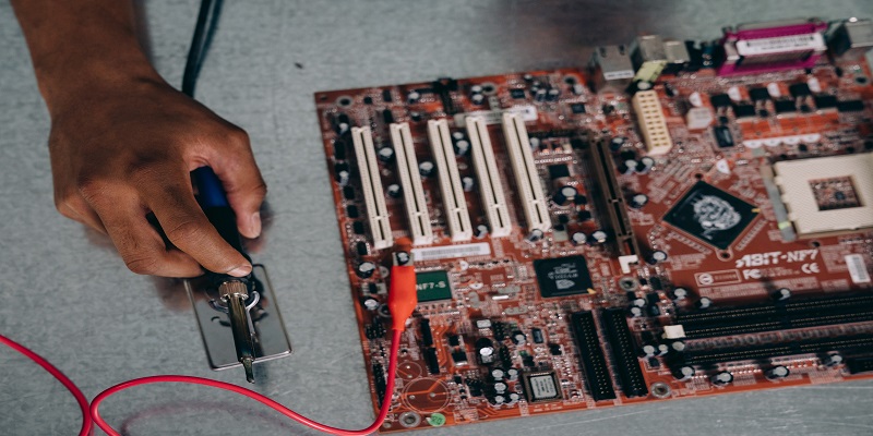
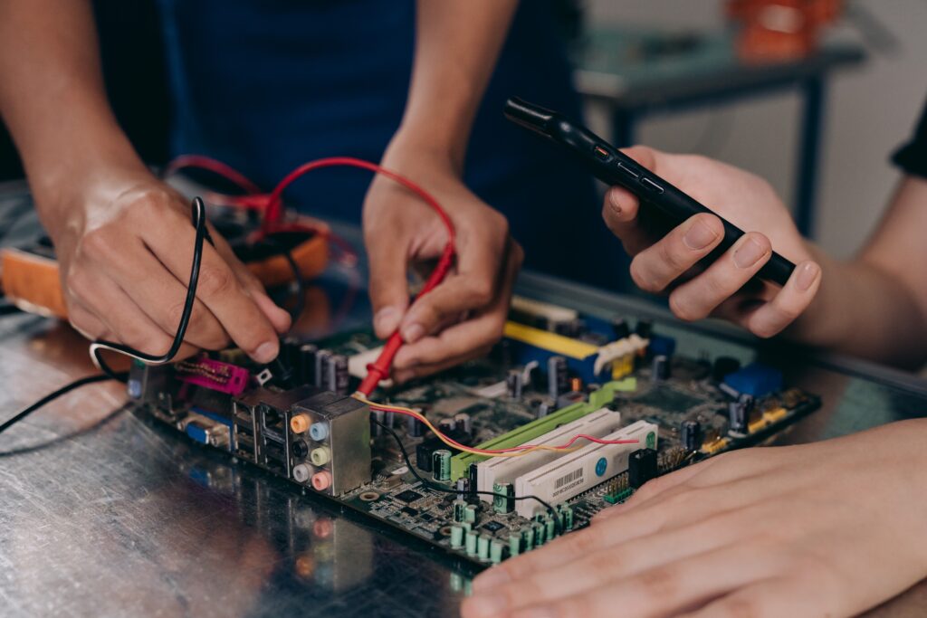
Unlike pure silicon, most semiconductors are metallic in structure. However, in certain instances, their metalization can occur without any other impurities. Examples of such materials include bimetals, which are semiconductors made from a boron-copper alloy. During the invention of integrated circuits, advances in material science enabled the development of materials with better conductivity, durability, and electrical and optical properties. These materials are used in almost all aspects of electronics, as well as photovoltaic and optoelectronic applications.
Although some semiconductors can be created through the simple interference of electrons, others must undergo some process known as doping. This method involves exposing the semiconductor to an electric field, which excites electrons within the semiconductor, causing a change in their orbital paths. The excited states of the electrons become single particles, while the single particles align themselves into a regular configuration in a way that is called a doped semiconductor. A type of doped semiconductor has a unique property called electron banding, in which there are distinct bands of electrons, which are narrow in range and tend to align themselves into a regular pattern.
There are two types of holes in semiconductors, known as conductors and carriers. The holes in a Semiconductor can be either intrinsic or extrinsic, depending upon their formation. Intrinsic holes occur when a substance is made by bonding atoms together, while extrinsic holes occur when a substance forms through the interaction of electrons with another substance. Intrinsic holes can be holes that align themselves with other atoms, or they can be holes that form when atoms align themselves, or bond too strongly to the outer surface of the semiconductor. While many companies have discovered methods for creating holes, once a hole is formed, it is extremely difficult to repair the alignment without adding another material to repair the damage that was done.
The valence band is a semiconductor’s most important physical structure, as it is the one that determines the properties of the semiconductor, which includes its ability to conduct electricity, produce electric current, and retain energy. The valence band is made up of one or more dipoles, which are atoms that have a single positive charge, and one or more single negative charges. As the electrons move from a positive state to a negative one in a process called conduction, the valence band becomes occupied by holes, which makes them either polar or nonpolar in nature. Polar holes absorb more electrons, while non-polar holes tend to lose fewer electrons. Because these holes are created through the interaction of two electrons, some conduction band processes are actually made up of pure holes. There are some conduction bands that have a combination of holes, which is the basis for the modern-day use of semiconductors in electronic devices.