Ever wondered how those powerful Nvidia chips are actually made? It’s a pretty wild journey, from scribbling ideas on paper to getting the final product into our hands. Nvidia has become a huge name, especially with all the buzz around AI. They didn’t just stumble into this success; there’s a whole process behind how Nvidia chips are made that’s pretty interesting. Let’s break down what goes into creating these essential pieces of technology.
Key Takeaways
- Nvidia chips start as detailed abstract models, which are then turned into physical blueprints using special software.
- The actual making of the chips happens in factories that provide specific toolkits for designers to use.
- Nvidia uses a smart sorting method called ‘binning’ to make sure every chip, no matter its performance, gets used.
- They’ve built a whole system around their hardware, like the CUDA software, which makes it hard for others to compete.
- Newer Nvidia chips, like those based on the Blackwell architecture, have special parts built just for AI tasks, showing they plan ahead.
The Genesis Of NVIDIA Chip Design
It all starts with an idea, right? For NVIDIA, that idea is to build chips that can do amazing things, especially when it comes to AI and graphics. This initial phase is all about translating a complex vision into something a computer can understand. Think of it like sketching out a blueprint for a super-advanced machine before anyone even thinks about cutting metal.
Translating Vision Into Abstract Models
So, how do you get from "we need a chip that can do X" to actual code? It’s a bit like writing a very detailed story. Designers start with high-level goals, like how fast a certain task needs to be done or how much power it should use. Then, they break that down into smaller, more manageable pieces. This involves creating abstract models, which are essentially mathematical descriptions of the chip’s logic. It’s a way to represent the intended behavior without getting bogged down in the nitty-gritty physical details just yet. This stage is where the core functionality is defined, laying the groundwork for everything that follows. It’s a critical step because any mistakes here can ripple through the entire design process.
Architecting Logic Components
Once you have those abstract models, it’s time to build the actual "brains" of the chip. This is where the logic components are designed. Designers figure out the structure, or "microarchitecture," of these parts. They might design each component from scratch, or sometimes they’ll use pre-made building blocks, called "IP cores," that they license from other companies. It’s a bit like choosing between custom-made parts for a car or using off-the-shelf components. This process is iterative; designers constantly tweak and adjust, balancing performance needs with practical considerations like cost and how much space they have on the chip. They’re essentially figuring out how all these pieces will fit together and talk to each other. This is where the foundation for NVIDIA’s data center strategy really starts to take shape.
Validating Designs Through Simulation
Before you can even think about making a physical chip, you have to be absolutely sure the design works. This is where simulation comes in. Designers use special software to run tests on their virtual chip design. It’s like running a thousand different scenarios in a video game to see if your character can handle every challenge. They check for errors, make sure it behaves as expected, and verify that it meets all the initial requirements. This simulation process is incredibly important because fixing a design flaw after the chip is made is extremely difficult and expensive. It’s all about catching problems early, saving time and a lot of headaches down the line. This rigorous testing is a hallmark of creating advanced hardware like the Blackwell Ultra GPU.
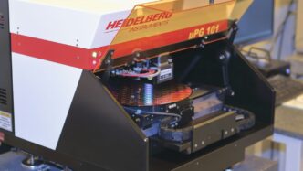
From Blueprint To Silicon: Fabrication And Assembly
So, you’ve got this amazing chip design, right? It’s all lines of code and logic on a screen. But how does that actually turn into the physical thing you can hold? It’s a pretty wild journey, honestly. It starts with these super-pure silicon wafers, like giant, shiny discs. Think of them as the canvas for our chip art.
The Role Of Process Design Kits
Before anyone can even start making chips, the fabrication plant, or ‘fab’, gives chip designers something called a Process Design Kit, or PDK. It’s basically a big instruction manual for designing chips that will work with that specific fab’s machinery and processes. Without the PDK, a design might look great on paper but would be impossible to actually build. It contains all the rules and details about the materials, the layers, and how everything needs to be laid out. This kit is what bridges the gap between the abstract design and the physical reality of silicon. It’s pretty detailed, covering everything from the size of transistors to how they connect.
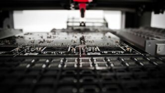
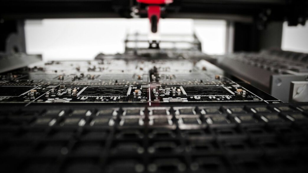
Leveraging Outsourced Semiconductor Assembly
Once the wafers are all patterned and cut into individual chips, they aren’t quite ready for prime time. They need to be assembled, tested, and packaged. A lot of this work happens at specialized facilities that focus just on this part, often called outsourced semiconductor assembly and test (OSAT). This is where the tiny silicon dies get put into protective casings, have connectors added, and are put through rigorous testing. Advanced packaging techniques, like CoWoS technology, are becoming super important here. They allow multiple chips or ‘chiplets’ to be combined in a single package, which is a big deal for performance. It’s not just about protecting the chip anymore; it’s about how they work together. This is a big part of why chip assembly and connectivity are so critical for overall performance these days.
The Binning Approach To Chip Sorting
Not every chip that comes off the production line is perfect. During the testing phase, chips are sorted based on their performance. This process is called ‘binning’. Chips that perform exceptionally well, maybe running at higher speeds or with fewer errors, get sorted into the ‘high-end’ bins. Those that meet a certain standard but aren’t top-tier go into other bins for different products. It’s a way to make sure that every chip finds a suitable home, whether it’s in a high-performance data center GPU or a more mainstream graphics card. This sorting is pretty important for getting the most out of the manufacturing process and making sure customers get a chip that meets their needs.
NVIDIA’s Strategic Advantage In Chip Production
NVIDIA didn’t just stumble into its current position; it’s the result of some really smart, long-term planning. While other companies were focused on small upgrades, NVIDIA saw the bigger picture: GPUs could do way more than just games. They could power AI, self-driving cars, and a whole lot more. This foresight, combined with tight control over their chip designs, has built a technological lead that just keeps growing.
Building An Ecosystem Around Hardware
One of the cleverest moves NVIDIA made was creating the CUDA software platform. Think of it as the main language for programming AI applications on their GPUs. They made CUDA free to use, but here’s the catch: it only works with NVIDIA hardware. This has built a huge community of developers who are now pretty much tied to using NVIDIA chips. Once a company invests in building its AI systems with CUDA, switching to a different chip maker becomes a really complicated and expensive headache. It’s a smart way to keep customers close. This approach has helped them build a robust and expanding supply chain moat for the company [2a53].
Acquisitions For Supply Chain Control
NVIDIA also thinks ahead by buying up key parts of the supply chain. A big example was their purchase of Mellanox back in 2020. Mellanox made high-speed networking gear, which is super important for connecting thousands of GPUs in those massive AI training systems. Instead of letting someone else control such a critical piece of the puzzle, NVIDIA brought it in-house. This lets them fine-tune how data moves between their GPUs, giving them an edge that’s hard for others to match. Their supply chain rapidly scaled to meet global demand, demonstrating resilience and adaptability [7848].
The Binning Approach To Chip Sorting
How NVIDIA handles chip production itself is pretty unique. Most chip companies try to get the most perfect chips out of every batch. NVIDIA, however, uses what they call the "binning approach." Basically, when a batch of chips is made, they test each one and sort them based on how well they perform. The absolute best chips go to data centers where speed is everything. Chips that are almost perfect but not quite make great gaming GPUs. Even chips with more noticeable flaws can find a home in car systems or less demanding products. This sorting method turns what others might consider manufacturing waste into a strategic advantage, making sure every chip has a purpose.
The Evolution Of NVIDIA’s AI Chip Technology
NVIDIA didn’t just stumble into the AI chip game; they saw it coming. While others were focused on making video game graphics look a little bit better, NVIDIA started thinking bigger. They realized that the powerful processors they were building for games, called GPUs, could actually be used for a lot more. This was a pretty big bet, but it paid off. NVIDIA’s long-term view has really changed how we think about computers today.
Specialized Circuits For New AI Models
As AI models get more complex, the chips need to keep up. NVIDIA is constantly designing new chips with specific parts built just for these new AI tasks. Think of it like needing a special tool for a very specific job. For example, their latest chips have circuits made to handle the kind of math that new AI models use a lot. This means they can do these AI jobs much faster and more efficiently than older chips.
Breaking Barriers In Accelerated Computing
Accelerated computing is basically using specialized hardware, like GPUs, to speed up tasks that regular computer processors struggle with. AI is a prime example. NVIDIA’s chips have been key in making AI training and running much faster. This has allowed researchers and companies to build and use AI models that were previously too slow or too difficult to work with. It’s like going from a bicycle to a race car for doing complex calculations.
The Blackwell Architecture’s Impact
The Blackwell architecture is the latest big step. It’s designed to be the engine for the next wave of AI, especially for things like AI reasoning. Compared to older generations, Blackwell chips can handle AI tasks way faster and use less power. For instance, the new GeForce RTX 50 Series GPUs, which use Blackwell, are about 4.5 times faster for AI tasks and use 30% less energy. This kind of progress is what allows for bigger and more capable AI systems to be built, pushing the boundaries of what’s possible. It’s a big deal for anyone working with large-scale AI, and it shows how NVIDIA is always looking ahead to what AI will need next. You can see how this technology has grown from their early days in computer gaming.
Understanding The Core Components Of NVIDIA Chips
So, what exactly makes an NVIDIA chip tick? It’s not just one thing, but a combination of specialized parts working together. At the heart of most of their powerful processors are the Graphics Processing Units, or GPUs. While they started out for gaming, these have become the workhorses for AI tasks. Think of them as massively parallel processors, meaning they can do a ton of calculations all at once, which is perfect for the kind of math AI models need.
Graphics Processing Units As AI Workhorses
NVIDIA’s GPUs are designed with a specific architecture that’s really good at handling the kind of computations common in deep learning. Unlike traditional CPUs that are good at handling a few complex tasks sequentially, GPUs have thousands of smaller cores that can tackle many simple tasks simultaneously. This parallel processing power is what makes them so effective for training and running AI models. Early on, NVIDIA saw that these chips could do more than just render graphics, and they’ve been refining them for AI ever since. You can find details on the architecture of some of their key GPUs, like the V100, A100, and H100, to get a better sense of how they’re built for this advanced hardware components.
High-Bandwidth Memory Integration
Next up, we have High-Bandwidth Memory, or HBM. This isn’t your typical RAM. HBM is stacked vertically and placed very close to the GPU itself. This proximity and design allow for incredibly fast data transfer between the memory and the processing cores. Imagine trying to feed a super-fast chef ingredients through a tiny straw versus having them right on the counter – HBM is like having the ingredients right there. This speed is super important because AI models often need to access huge amounts of data very quickly. For example, the H100 accelerator often features six surrounding HBM chips, all working together to keep the GPU fed with data.
The Function Of Tensor Operations
Finally, let’s talk about Tensor Cores. These are specialized processing units within NVIDIA GPUs that are specifically designed to speed up matrix multiplication and other tensor operations. These operations are the backbone of deep learning algorithms. By having dedicated hardware for these calculations, NVIDIA chips can perform AI tasks much faster and more efficiently than if they had to rely solely on general-purpose cores. Newer architectures, like the Blackwell series, have even more advanced Transformer Engines that further accelerate these critical AI computations, supporting new precisions and improving performance for large language models. This focus on specialized operations is a big reason why NVIDIA has become so dominant in the AI space, even offering processors like the NVIDIA Grace for specific high-performance computing needs.
The Road Ahead
So, that’s a look at how these powerful NVIDIA chips go from an idea to something you can actually hold. It’s a seriously complex journey, involving a ton of smart people and some really advanced tech. From the initial design sketches to the massive factories churning out wafers, it’s a whole world of engineering. And it’s not like they just make one chip and call it a day; they’re always working on the next big thing, trying to make things faster and better. It really makes you appreciate the effort that goes into the technology we often take for granted.
Frequently Asked Questions
How does NVIDIA come up with the ideas for new chips?
NVIDIA engineers start by thinking about what future computer tasks will need. They then create a detailed plan, like a blueprint, for the chip’s circuits. This plan is checked and tested using special computer programs to make sure it works correctly before the chip is actually made.
What is the ‘binning approach’ NVIDIA uses?
The ‘binning approach’ is a smart way NVIDIA sorts chips after they are made. The best chips, which work the fastest, are used for powerful computers. Chips that are good but not perfect are used for things like gaming. Even chips with small flaws can be used in cars or other products. This way, fewer chips are wasted.
Why are NVIDIA’s GPUs so good for AI?
GPUs, or Graphics Processing Units, are great at doing many math problems at the same time. AI tasks, especially those involving learning from lots of data, need a lot of math done quickly. NVIDIA’s GPUs are designed to handle these kinds of calculations very efficiently, making them perfect for AI.
What is the Blackwell architecture?
The Blackwell architecture is the latest design for NVIDIA’s AI chips. It’s built to be much faster and more efficient than older designs. It includes special parts made specifically to handle new and complex AI tasks, helping to push the boundaries of what AI can do.
How does NVIDIA work with other companies to make chips?
NVIDIA designs its chips but usually doesn’t make them in its own factories. Instead, they send their designs to special factories called ‘fabs’ that specialize in manufacturing chips. These fabs use detailed instructions provided by NVIDIA, called a Process Design Kit (PDK), to create the actual silicon.
What is High-Bandwidth Memory (HBM) and why is it important?
High-Bandwidth Memory (HBM) is a special type of computer memory that works very quickly and is placed very close to the main chip, like the GPU. This allows the chip to access data much faster, which is crucial for demanding tasks like AI training and graphics processing where speed is essential.